


TMP92CM22
2007-02-16
92CM22-206
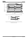
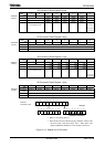
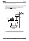
3.11.2 Description of Operation
(1) Analog reference voltage
A high-level analog reference voltage is applied to the VREFH pin; a low-level analog
reference voltage is applied to the VREFL pin. To perform AD conversion, the reference
voltage, the difference between VREFH and VREFL, is divided by 1024 using string
resistance. The result of the division is then compared with the analog input voltage.
To turn off the switch between VREFH and VREFL, program a 0 to
ADMOD1<VREFON> in AD mode control register 1. To start AD conversion in the
OFF state, first write a 1 to ADMOD1<VREFON>, wait 3 μs until the internal
reference voltage stabilizes (This is not related to f
SYS
), then set ADMOD0<ADS> to 1.
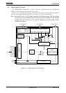
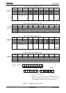
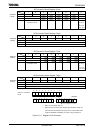
(2) Analog input channel selection
The analog input channel selection varies depends on the operation mode of the AD
converter.
• In analog input channel fixed mode (ADMOD0<SCAN> = 0)
Setting ADMOD1<ADCH2:0> selects one of the input pins AN0 to AN7 as the input
channel.
• In analog input channel scan mode (ADMOD0<SCAN> = 1)
Setting ADMOD1<ADCH2:0> selects one of the eight scan modes.
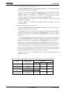
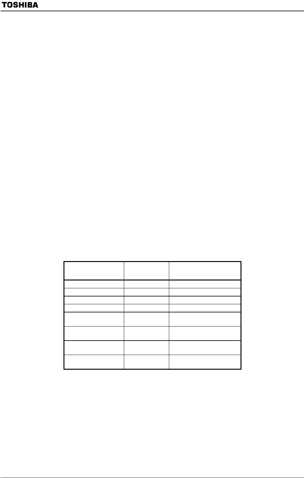
Table 3.11.1 illustrates analog input channel selection in each operation mode.
On a reset, ADMOD0<SCAN> is set to “0” and ADMOD1<ADCH2:0> is initialized to
“000”. Thus pin AN0 is selected as the fixed input channel. Pins not used as analog
input channels can be used as standard input port pins.
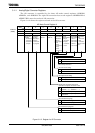
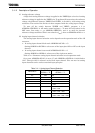
Table 3.11.1 Analog Input Channel Selection
<ADCH2:0>
Channel fixed
<SCAN> = “0”
Channel scan
<SCAN> = “1”
000 AN0 AN0
001 AN1 AN0 → AN1
010 AN2 AN0 → AN1 → AN2
011 AN3 AN0 → AN1 → AN2 → AN3
100 AN4 AN0 → AN1 → AN2 → AN3
→ AN4
101 AN5 AN0 → AN1 → AN2 → AN3
→ AN4 → AN5
110 AN6 AN0 → AN1 → AN2 → AN3
→ AN4 → AN5 → AN6
111 AN7 AN0 → AN1 → AN2 → AN3
→ AN4 → AN5 → AN6 → AN7