


TMP92CM22
2007-02-16
92CM22-12
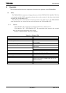
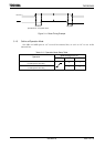
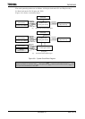
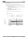
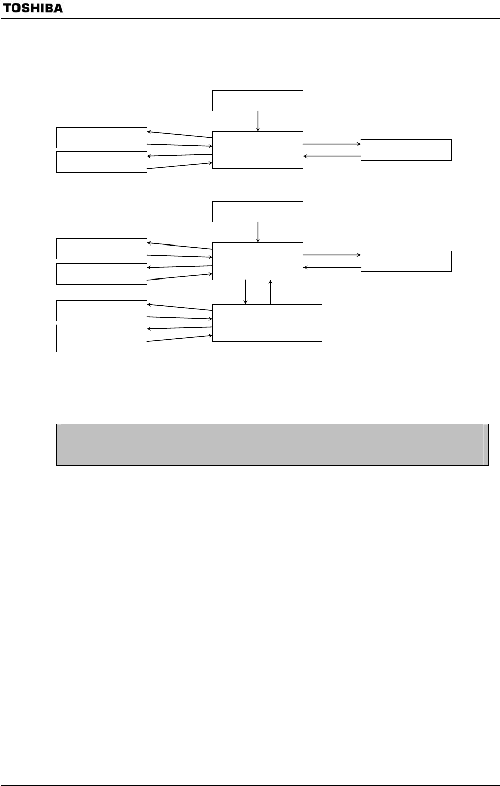
The clock operating modes are as follows: (a) Single clock mode (X1 and X2 pins only),
(b) Dual clock mode (X1, X2 pins and PLL).
Figure 3.3.1 shows a transition figure.
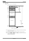
Figure 3.3.1 System Clock Block Diagram
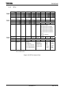
The clock frequency input from the X1 and X2 pins is called f
OSCH
and the clock frequency selected by
SYSCR1<GEAR2:0> is called the clock f
FPH
. The system clock f
SYS
is defined as the divided 2 clocks of f
FPH
, and
one cycle of f
SYS
is defined to as one state.
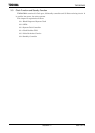
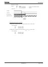
Reset
(f
OSCH
/32)
NORMAL mode
(f
OSCH
/gear value/2)
IDLE2 mode
(I/O operation)
IDLE1 mode
(Operate only oscillator)
Interrupt
Instruction
Interrupt
Instruction
Release reset
Interrupt
Instruction
STOP mode
(Stop all circuit )
(a) Single clock mode transition figure
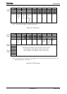
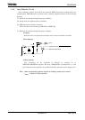
(b) Dual clock mode transition figure
Reset
(f
OSCH
/32)
NORMAL mode
(f
OSCH
/gear value/2)
Release reset
Interrupt
Instruction
STOP mode
(Stop all circuit )
NORMAL mode
(4 × f
OSCH
/gear value/2)
IDLE2 mode
(
I/O o
p
eration
)
IDLE1 mode
(Operate only oscillator)
Interrupt
Instruction
Interrupt
Instruction
IDLE2 mode
(I/O operation)
IDLE1 mode
(Operate
oscillator and PLL )
Interrupt
Instruction
Interrupt
Instruction
(Using PLL)
Instruction