


TMP92CM22
2007-02-16
92CM22-156
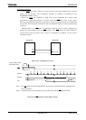
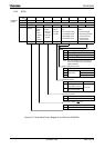
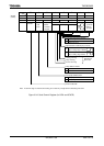
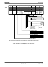
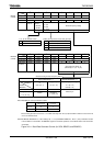
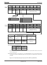
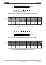
7 6 5 4 3 2 1 0
Bit symbol RB8 EVEN PE OERR PERR FERR SCLKS IOC SC0CR
(1201H)
Read/Write R R/W R (Cleared to 0 when read) R/W
After reset Undefined 0 0 0 0 0 0 0
Function 1: Error
Received
data bit8
Parity
0: Odd
1: Even
Parity
addition
0: Disable
1: Enable
Overrun Parity Framing
0: SCLK0
1: SCLK0
0: Baud rate
generator
1: SCLK0
pin input
0 Baud rate generator
1 SCLK0 pin input
0
Transmits and receivers
data on rising edge of SCLK0.
1
Transmits and receivers
data on falling edge SCLK0.
0 Disabled
1 Enabled
0 Odd parity
1 Even parity
Note: As all error flags are cleared after reading, do not test only a single bit with a bit-testing instruction.
Figure 3.9.9 Serial Control Register (for SIO0 and SC0CR)
I/O interface input clock selection
Edge selection for SCLK0 pin (I/O mode)
Framing error flag
Parity error flag
Overrun error flag
Parity addition enables
Even parity addition/check
Received data bit8
Cleared to 0
when read