


TMP92CM22
2007-02-16
92CM22-91
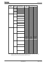
3.6.5 List of Registers
The memory control registers and the settings are described as follows. For the
addresses of the registers, see list of special function registers in section 5.
(1) Control registers
The control register is a pair of BnCSL and BnCSH. (“n” is a number of the block
address area.) BnCSL has the same configuration regardless of the block address
areas. In BnCSH, only B2CSH which is corresponded to the block address area 2 has a
different configuration from the others.
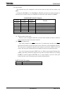
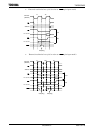
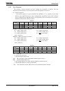
BnCSL
7 6 5 4 3 2 1 0
Bit symbol BnWW2 BnWW1 BnWW0 BnWR2 BnWR1 BnWR0
Read/Write W W
After reset 0 1 0 0 1 0
BnWW[2:0] Specifies the number of write waits.
001 = 2 states (0 waits) access 010 = 3 states (1 wait) access
101 = 4 states (2 waits) access 110 = 5 states (3 waits) access
111 = 6 states (4 waits) access 011 =
WAIT pin input mode
Others = (Reserved)
BnWR[2:0] Specifies the number of read waits.
001 = 2 states (0 waits) access 010 = 3 states (1 wait) access
101 = 4 states (2 waits) access 110 = 5 states (3 waits) access
111 = 6 states (4 waits) access 011 =
WAIT pin input mode
Others = (Reserved)
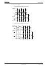
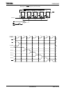
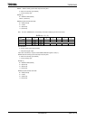
B2CSH
7 6 5 4 3 2 1 0
Bit symbol B2E B2M B2REC B2OM1 B2OM0 B2BUS1 B2BUS0
Read/Write W W
After reset 1 0 0 0 0 0 0
B2E Enable bit.
0 = No chip select signal output
1 = Chip select signal output (Default)
Note: After reset release, only the enable bit B2E of B2CSH register is valid (“1”).
B2M Specifies the block address area.
0 = Sets the block address area of CS2 to addresses 000000H to FFFFFFH (Default)
1 = Sets the block address area of CS2 to programmable
Note: After reset release, the block address area 2 is set to addresses 000000H to FFFFFFH.