


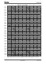


TMP92CM22
2007-02-16
92CM22-104
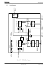
(4) Comparator (CP0)
The comparator compares the value in an up counter with the value set in a timer
register. If they match, the up counter is cleared to 0 and an interrupt signal (INTTA0
or INTTA1) is generated. If timer flip-flop inversion is enabled, the timer flip-flop is
inverted at the same time.
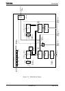
(5) Timer flip-flop (TA1FF)
The timer flip-flop (TA1FF) is a flip-flop inverted by the match detects signal (8-bit
comparator output) of each interval timer.
Whether inversion is enabled or disabled is determined by the setting of the bit
TA1FFCR<TA1FFIE> in the timer flip-flops control register. A reset clears the value of
TA1FF to “0”. Programming “01” or “10” to TA1FFCR<TA1FFC1:0> sets TA1FF to 0 or
1. Programming “00” to these bits inverts the value of TA1FF. (This is known as
software inversion.)
The TA1FF signal is output via the TA1OUT pin (which can also be used as PC1).
When this pin is used as the timer output, the timer flip-flop should be set beforehand
using the port C function register PCFC.
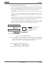
Note: When the double buffer is enabled for an 8-bit timer in PWM or PPG mode, caution is required
as explained below.
If new data is written to the register buffer immediately before an overflow occurs by a
match between the timer register value and the up-counter value, the timer flip-flop may
output an unexpected value.
For this reason, make sure that in PWM mode new data is written to the register buffer by
six cycles (f
SYS
× 6) before the next overflow occurs by using an overflow interrupt.
When using PPG mode, make sure that new data is written to the register buffer by six
cycles before the next cycle compare match occurs by using a cycle compare match
interrupt.
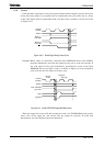
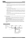
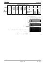
Example when using PWM mode
TA1OUT
2
n
overflow interrupt
(INTTA0)
t
PWM
(PWM cycle)
Match between
TA0REG and up-counter
Desired PWM cycle
change point
Write new data to the register buffer
before the next overflow occurs by
using an overflow interrupt