


TMP92CM22
2007-02-16
92CM22-92
B2REC Sets the dummy cycle for data output recovery time.
0 = Not insert a dummy cycle (Default)
1 = Insert a dummy cycle
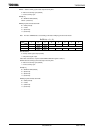
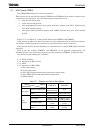
B2OM[1:0]
00 = SRAM or ROM (Default)
Others = (Reserved)
B2BUS[1:0] Sets the data bus width.
00 = 8 bits (Default)
01 = 16 bits
10 = (Reserved)
11 = (Reserved)
Note: The value of B2BUS bit is set according to the state of AM[1:0] pin after reset release.
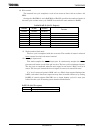
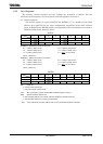
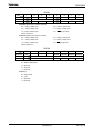
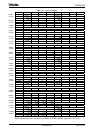
BnCSH (n = 0, 1, 3)
7 6 5 4 3 2 1 0
Bit symbol BnE BnREC BnOM1 BnOM0 BnBUS1 BnBUS0
Read/Write W W
After reset 0 0 0 0 0 0
BnE Enable bit.
0 = No chip select signal output (Default)
1 = Chip select signal output
Note: After reset release, only the enable bit B2E of B2CSH register is valid (“1”).
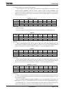
BnREC Sets the dummy cycle for data output recovery time.
0 = Not insert a dummy cycle (Default)
1 = Insert a dummy cycle
BnOM[1:0]
00 = SRAM or ROM (Default)
01 = (Reserved)
10 = (Reserved)
11 = (Reserved)
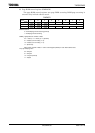
BnBUS[1:0] Sets the data bus width.
00 = 8 bits (Default)
01 = 16 bits
10 = (Reserved)
11 = (Reserved)