


TMP92CM22
2007-02-16
92CM22-57
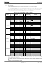
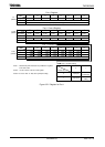
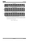
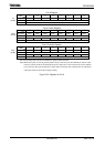
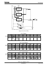
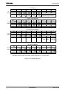
Port 5 Register
7 6 5 4 3 2 1 0
Bit symbol P57 P56 P55 P54 P53 P52 P51 P50
Read/Write R/W
After reset Data from external port (Output latch register is cleared to “0”.)
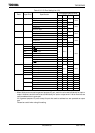
Port 5 Control Register
7 6 5 4 3 2 1 0
Bit symbol P57C P56C P55C P54C P53C P52C P51C P50C
Read/Write W
After reset 0 0 0 0 0 0 0 0
Function 0: Input 1: Output (Note2)
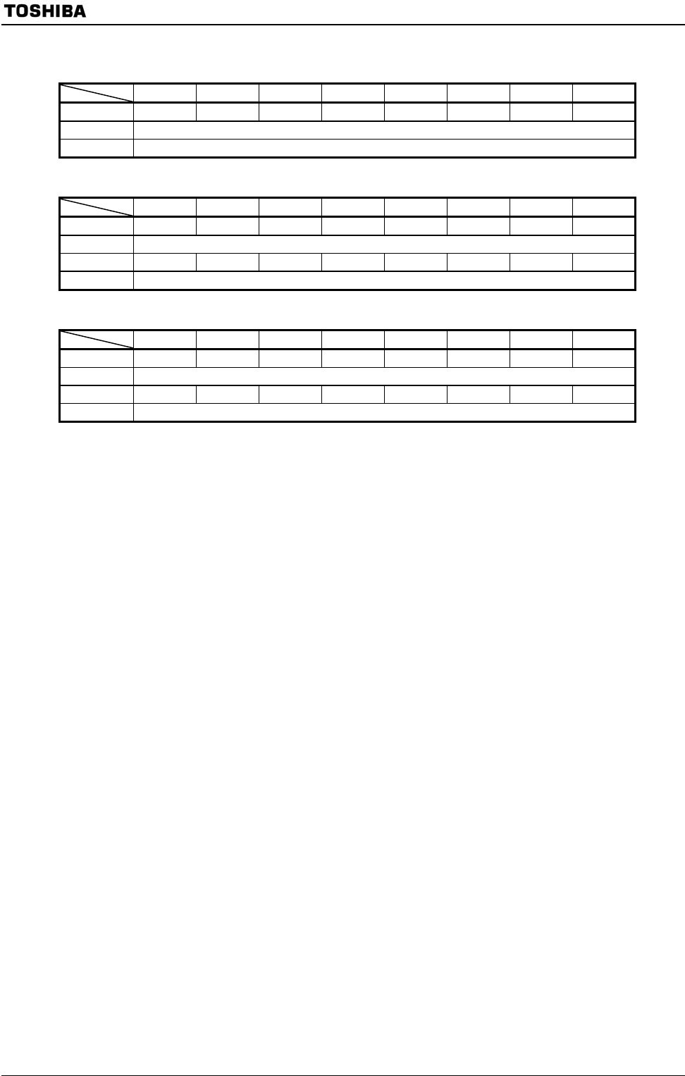
Port 5 Function Register
7 6 5 4 3 2 1 0
Bit symbol P57F P56F P55F P54F P53F P52F P51F P50F
Read/Write W
After reset 1 1 1 1 1 1 1 1
Function 0: Port 1: Address bus (A8 to A15)
Note1: Read-modify-write instruction is prohibited for registers P5CR and P5FC.
Note2: When these ports are used as general-purpose I/O port, each bit can be set individually for input or output.
However, each bit cannot be set individually for input or output even if 1bit or more bits are used as address
bus in same port. All of general-purpose I/O ports except for port that used as address bus are operated as
output port. Please be careful when using this setting.
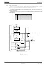
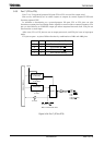
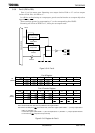
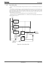
Figure 3.5.6 Register for Port 5
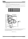
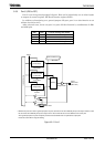
P5
(0014H)
P5CR
(0016H)
P5FC
(0017H)