


TMP92CM22
2007-02-16
92CM22-153
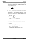
2. Parity error <PERR>
The parity generated for the data shifted into receiving buffer 2 (SC0BUF) is
compared with the parity bit received via the RXD pin. If they are not equal, a
parity error is generated.
3. Framing error <FERR>
The stop bit for the received data is sampled three times around the center. If
the majority of the samples are 0, a framing error is generated.
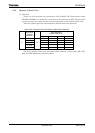
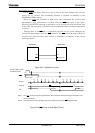
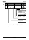
(12) Timing generation
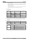
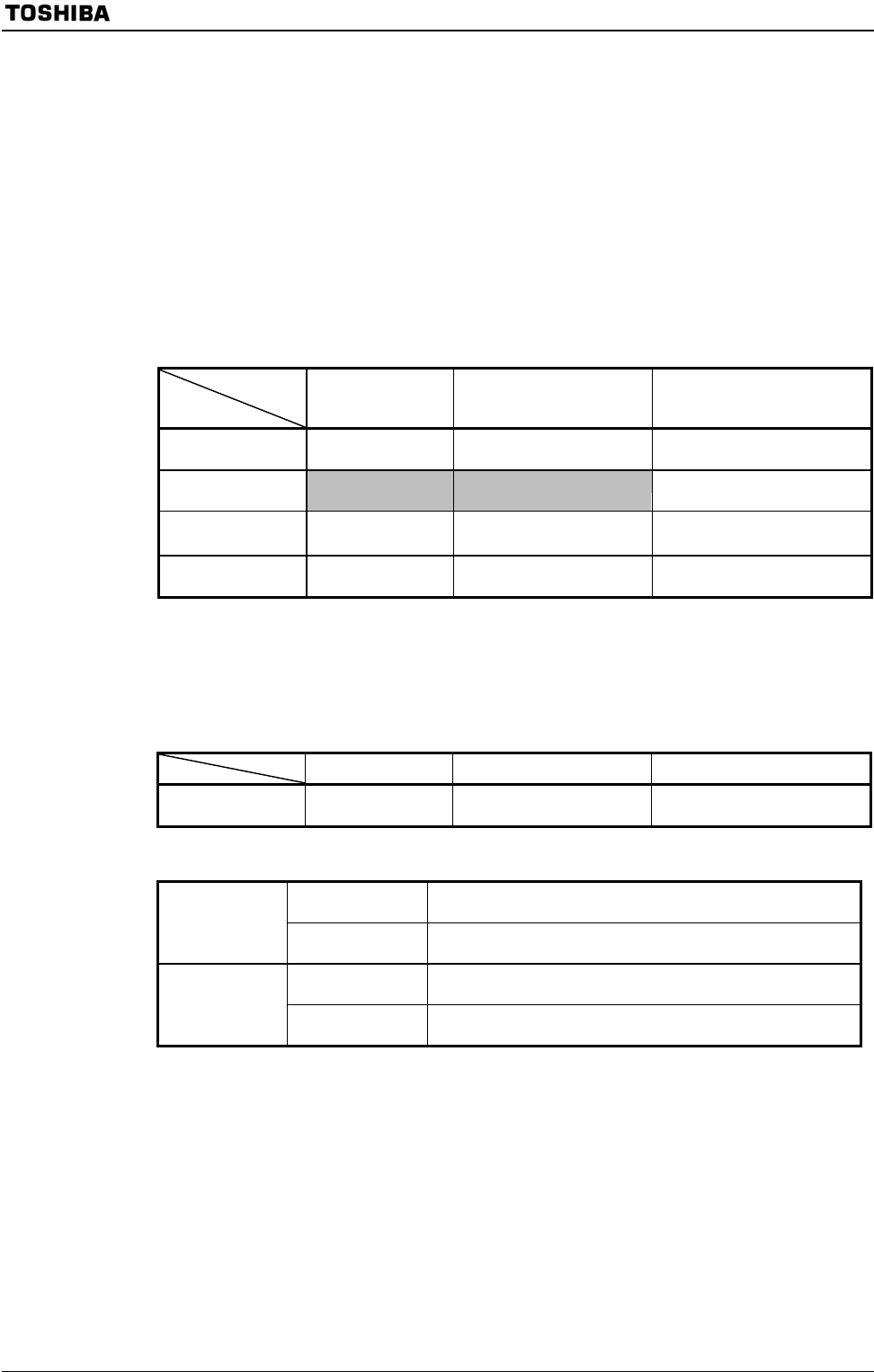
1. In UART mode
Receiving
Mode
9 Bits 8 Bits + Parity 8 Bits, 7 Bits + Parity, 7 Bits
Interrupt generation
timing
Center of last bit
(Bit8)
Center of last bit
(Parity bit)
Center of stop bit
Framing error
generation timing
Center of stop bit Center of stop bit Center of stop bit
Parity error
generation timing
−
Center of last bit
(Parity bit)
Center of stop bit
Overrun error
generation timing
Center of last bit
(Bit8)
Center of last bit
(Parity bit)
Center of stop bit
Note1: In 9 Bits mode and 8 Bits + Parity mode, interrupts coincide with the ninth bit pulse. Thus, when servicing the
interrupt, it is necessary to wait for a 1-bit period (to allow the stop bit to be transferred) to allow checking for
a framing error.
Note2: The higher the transfer rate, the later than the middle receive interrupts and errors occur.
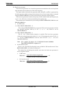
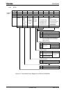
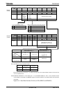
Transmission
Mode
9 Bits 8 Bits + Parity 8 Bits, 7 Bits + Parity, 7 Bits
Interrupt generation
timing
Just before stop bit is
transmitted
← ←
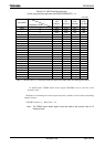
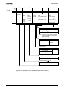
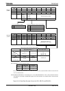
2. In I/O interface mode
SCLK output mode Immediately after last bit data.
(See
Figure 3.9.19.)
Transmission
interrupt
timing
SCLK input mode Immediately after rise of last SCLK signal rising mode, or
immediately after fall in falling mode. (See
Figure 3.9.20.)
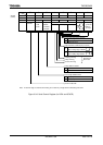
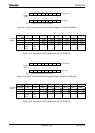
SCLK output mode Timing used to transfer received to data receive buffer 2 (SC0BUF)
(e.g., immediately after last SCLK). (See
Figure 3.9.21.)
Receiving
interrupt
timing
SCLK input mode Timing used to transfer received data to receive buffer 2 (SC0BUF)
(e.g., immediately after last SCLK). (See
Figure 3.9.22.)