


TMP92CM22
2007-02-16
92CM22-129
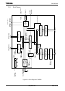
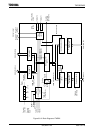
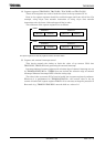
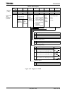
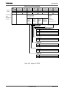
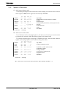
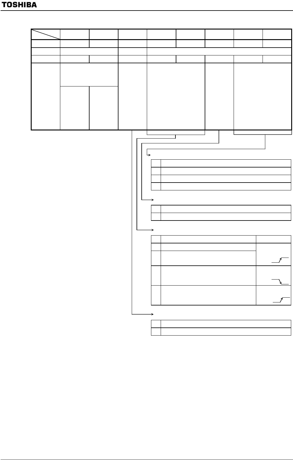
TMRB1 Mode Register
7 6 5 4 3 2 1 0
Bit symbol TB1CT1 TB1ET1 TB1CP0I TB1CPM1 TB1CPM0 TB1CLE TB1CLK1 TB1CLK0TB1MOD
(1192H)
Read/Write R/W W R/W
After reset 0 0 1 0 0 0 0 0
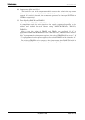
TB1FF1 Inversion trigger
0: Trigger disable
1: Trigger enable
Function
Invert when
UC12 is
loaded into
TB1CP1H/L
Invert when
UC12
matches
with
TB1RG1H/L
Software
capture
control
0: Software
capture
1: Undefined
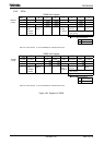
Capture timing
00: Disable
INT4 is rising edge
01: TB1N0 ↑ TB1IN1 ↑
INT4 is falling edge
10: TB1IN0 ↑ TB1IN0 ↓
INT4 is falling edge
11: TA1TRG ↑
TA1TRG ↓
INT4 is rising edge
Up counter
control
0: Clear
disable
1: Clear
enable
TMRB1 source clock
00: TB1IN0 pin input
01: φT1
10: φT4
11: φT16
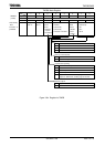
00 TB1IN0 pin input
01 φT1
10 φT4
11 φT16
0 Clear disable
1 Clear by matching with TB1RG1H/L
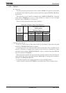
Capture control INT4 control
00 Capture disable
01 Capture to TB1CP0H/L at rising edge of TB1IN0
Capture to TB1CP1H/L at rising edge of TB1IN1
Generate INT4
by TB1IN0
rising
10 Capture to TB1CP0H/L at rising edge of TB1IN0
Capture to TB1CP1H/L at falling edge of TB1IN1
Generate INT4
by TB1IN0
falling
11 Capture to TB1CP0H/L at rising edge of TA1OUT
Capture to TB1CP1H/L at falling edge of TA1OUT
Generate INT4
by TB1IN0
rising
0 Capture value of up counter to TB1CP0H/L
1 Undefined
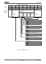
Figure 3.8.5 Register for TMRB
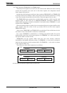
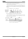
Input clock
Clear up counter (UC12)
Capture/interrupt timing
Software ca
p
ture
Read-modify
-write
instruction is
prohibited