


TMP92CM22
2007-02-16
92CM22-76
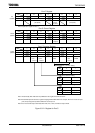
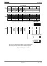
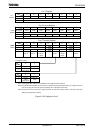
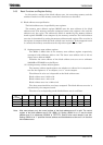
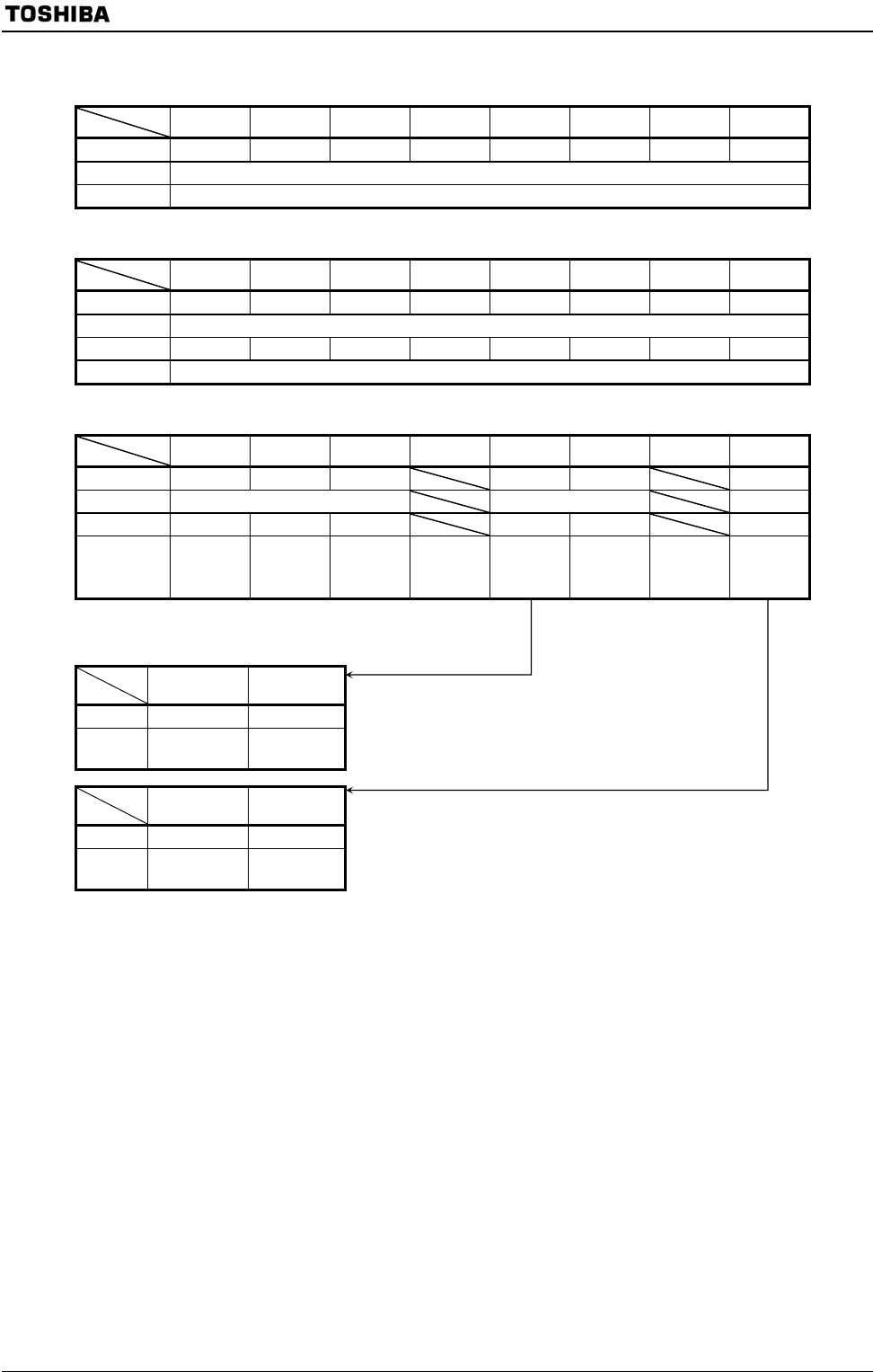
Port F Register
7 6 5 4 3 2 1 0
Bit symbol PF7 PF6 PF5 PF4 PF PF2 PF1 PF0
Read/Write R/W
After reset Data from external port (Output latch register is set to 1)
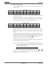
Port F Control Register
7 6 5 4 3 2 1 0
Bit symbol PF7C PF6C PF5C PF4C PF3C PF2C PF1C PF0C
Read/Write W
After reset 0 0 0 0 0 0 0 0
Function 0: Input 1: Output
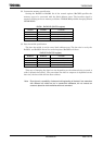
Port F Function Register
7 6 5 4 3 2 1 0
Bit symbol − − PF5F PF3F PF2F PF0F
Read/Write W W W
After reset 0 0 0 0 0 0
Function Always
write “0”.
Always
write “0”.
0: Port
1: SCLK1
output
0: Port
1: TXD1
0: Port
1: SCLK0
output
0: Port
1: TXD0
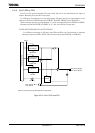
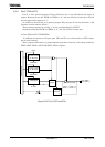
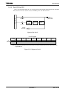
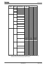
<PF3C>
<PF3F>
0 1
0 Input port Output port
1
TXD1
(Open drain)
TXD1
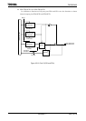
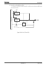
<PF0C>
<PF0F>
0 1
0 Input port Output port
1
TXD0
(Open drain)
TXD0
Note 1: Read-modify-write instruction is prohibited for the registers PFCR and PFFC.
Note 2: PF1/RXD0 and PF4/RXD1 pins do not have a register changing PORT/FUNCTION. For example, when it is
used as an input port, the input signal is inputted to SIO as the serial receive data.
Note 3: PF0 and PF3 pins do not have a register (PFODE) for open-drain setting. Please conduct the open-drain
setting according to above setting.
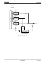
Figure 3.5.29 Register for Port F
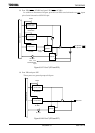
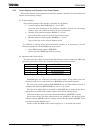
PFFC
(003FH)
PF
(003CH)
PFCR
(003EH)
PFCR
(003EH)
PFFC
(003FH)
Port function setting