


TMP92CM22
2007-02-16
92CM22-97
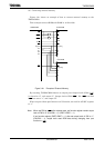
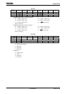
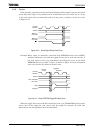
3.6.6 Caution
If the parasitic capacitance of the read signal (Output enable signal) is greater than that
of the chip select signal, it is possible that an unintended read cycle occurs due to a delay
in the read signal. Such an unintended read cycle may cause a trouble as in the case of (a)
in
Figure 3.6.3
Figure 3.6.3 Read Signal Delay Read Cycle
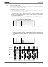
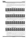
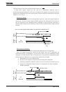
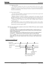
Example: When using an externally connected flash EEPROM which users JEDEC
standard commands, note that the toggle bit may not be read out correctly. If
the read signal in the cycle immediately preceding the access to the flash
EEPROM does not go “high” in time, as shown in
Figure 3.6.4 an unintended
read cycle like the one shown in (b) may occur.
Figure 3.6.4 Flash EEPROM Toggle Bit Read Cycle
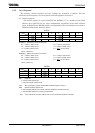
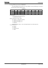
When the toggle bit reverse with this unexpected read cycle, TMP92CM22 always reads
same value of the toggle bit, and cannot read the toggle bit correctly. To avoid this
phenomenon, the data polling control recommended.
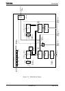
Memory 1
chip select
Memory 2
chip select
Address
CLKOUT
(20 MHz)
(a)
RD
Address
CLKOUT
(20 MHz)
Flash EEPROM
chip select
Read
(b)
Toggle bit
Memory
access
Toggle bit
RD cycle 1