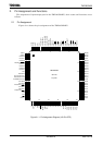
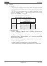
TMP92CM22
2007-02-16
92CM22-163
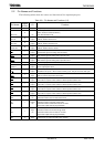
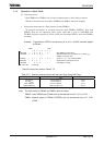
2. Receiving
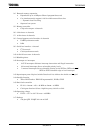
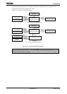
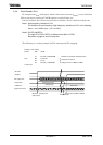
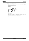
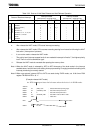
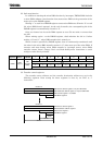
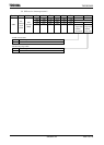
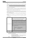
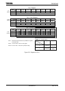
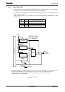
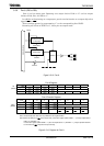
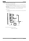
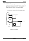
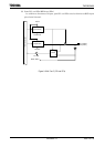
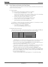
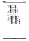
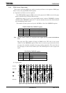
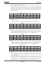
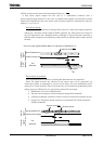
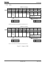
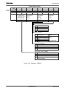
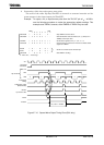
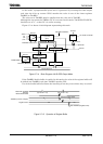
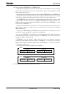
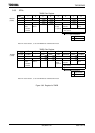
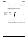
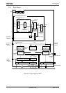
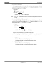
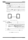
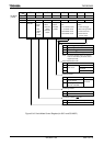
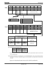
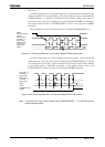
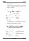
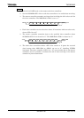
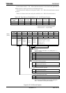
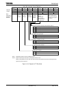
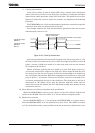
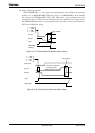
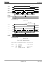
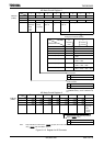
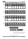
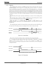
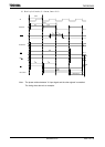
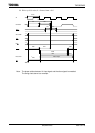
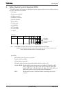
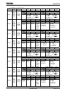
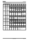
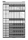
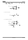
In SCLK output mode, the synchronous clock is outputted from SCLK0 pin and
the data is shifted to receiving buffer 1. This starts when the receive interrupt flag
INTES0<IRX0C> is cleared by reading the received data. When 8-bit data are
received, the data will be transferred to receiving buffer 2 (SC0BUF according to
the timing shown below) and INTES0<IRX0C> will be set to generate INTRX0
interrupt.
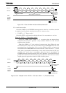
The outputting for the first SCLK0 starts by setting SC0MOD0<RXE> to 1.
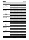
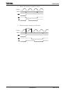
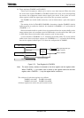
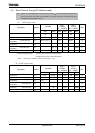
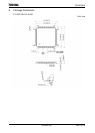
Figure 3.9.21 Receiving Operation in I/O Interface Mode (SCLK0 output mode)
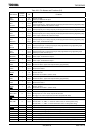
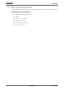
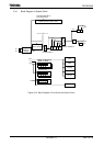
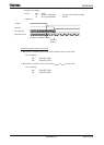
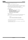
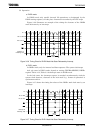
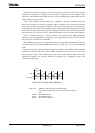
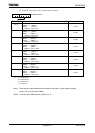
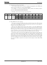
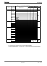
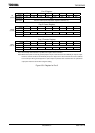
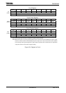
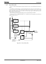
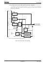
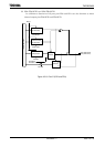
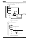
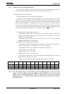
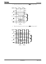
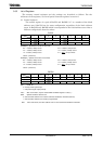
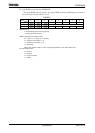
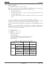
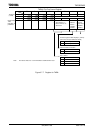
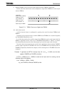
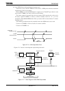
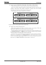
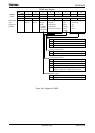
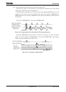
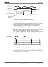
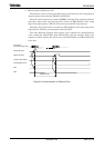
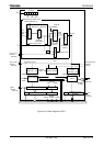
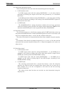
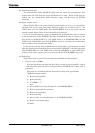
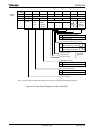
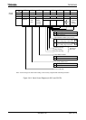
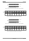
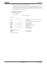
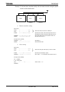
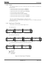
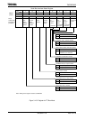
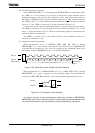
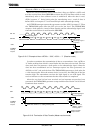
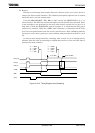
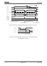
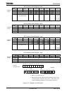
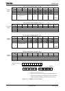
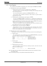
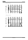
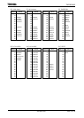
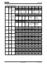
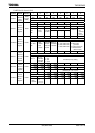
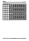
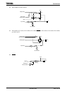
In SCLK input mode, the data is shifted to receiving buffer 1 when the SCLK
input becomes active after the receive interrupt flag INTES0<IRX0C> is cleared
by reading the received data. When 8-bit data is received, the data will be shifted
to receiving buffer 2 (SC0BUF according to the timing shown below) and
INTES0<IRX0C> will be set again to be generate INTRX0 interrupt.
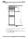
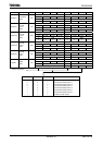
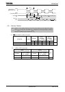
Figure 3.9.22 Receiving Operation in I/O Interface Mode (SCLK0 input mode)
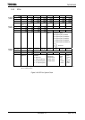
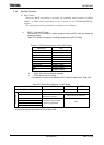
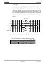
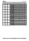
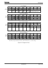
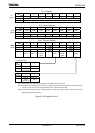
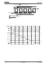
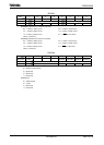
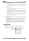
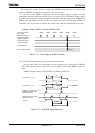
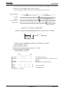
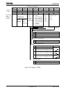
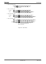
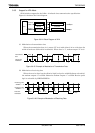
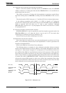
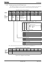
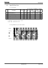
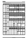
Note: If receiving, set to the receive enable state (SC0MOD0<RXE> = 1) in both SCLK input
mode and output mode.
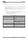
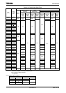
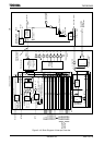
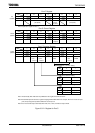
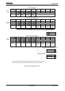
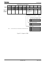
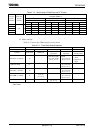
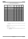
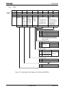
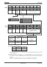
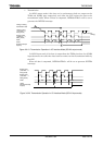
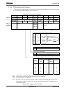
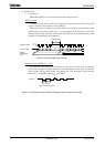
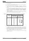
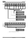
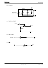
Bit0 Bit1 Bit6 Bit7 Bit5
SCLK0 input
(<SCLKS> = 0:
rising mode)
SCLK0 input
(<SCLKS> = 1:
falling mode)
RXD1
IRX0C
(INTRX0 interrupt
request)
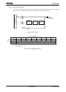
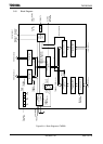
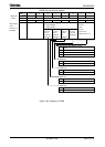
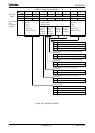
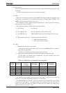
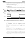
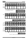
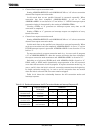
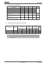
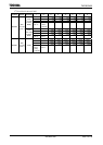
SCLK0 output
(<SCLKS> = 0:
rising mode)
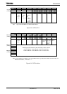
Bit7 Bit0 Bit1 Bit6
IRX0C
(INTRX0 interrupt
request)
RXD0
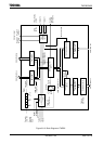
SCLK0 output
(<SCLKS> = 1:
falling mode)