


TMP92CM22
2007-02-16
92CM22-103
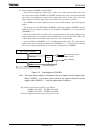
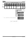
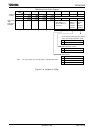
(3) Timer registers (TA0REG and TA1REG)
These are 8-bit registers, which can be used to set a time interval. When the value
set in the timer register TA0REG or TA1REG matches the value in the corresponding
up counter, the comparator match detect signal goes Active. If the value set in the
timer register is 00H, the signal goes active when the up counter overflows.
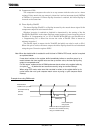
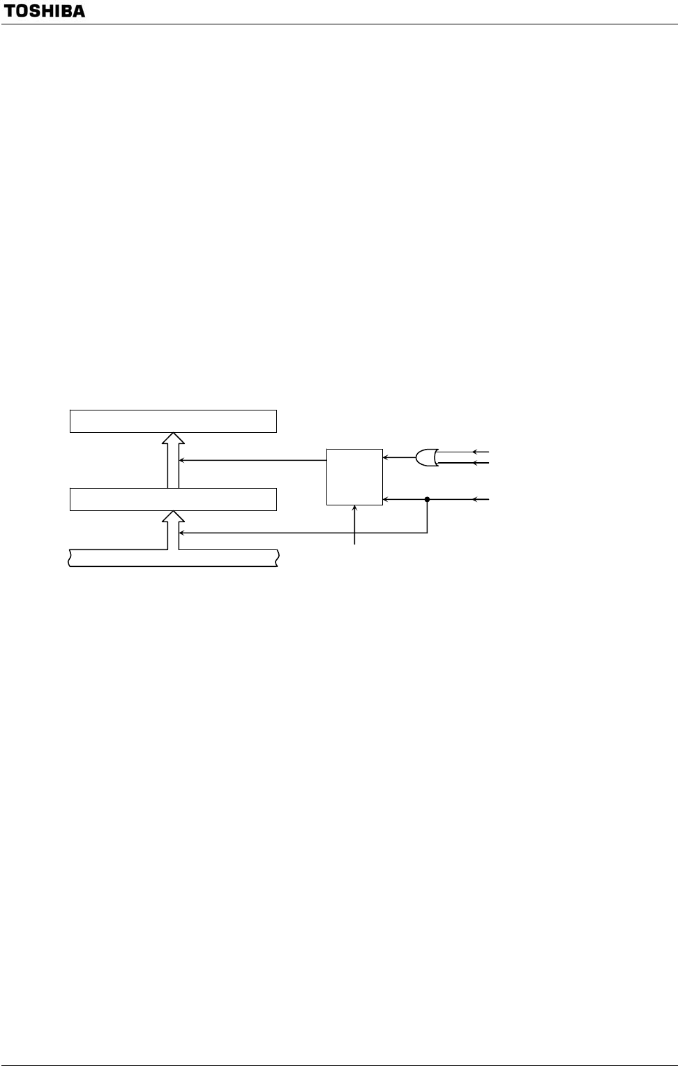
The TA0REG are double buffer structure, each of which makes a pair with register
buffer.
The setting of the bit TA01RUN<TA0RDE> determines whether TA0REG’s double
buffer structure is enabled or disabled. It is disabled if <TA0RDE> = “0” and enabled if
<TA0RDE> = “1”.
When the double buffer is enabled, data is transferred from the register buffer to the
timer register when a 2
n
overflow occurs in PWM mode, or at the start of the PPG cycle
in PPG mode. Hence the double buffer cannot be used in timer mode.
A reset initializes <TA0RDE> to “0”, disabling the double buffer. To use the double
buffer, write data to the timer register, set <TA0RDE> to “1”, and write the following
data to the register buffer
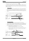
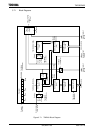
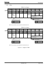
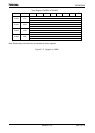
Figure 3.7.3 show the configuration of TA0REG
Figure 3.7.3 Timer Register A0 (TA0REG)
Note: The same memory address is allocated to the timer register and the register buffer.
When <TA0RDE> = 0, the same value is written to the register buffer and the timer
register; when <TA0RDE> = 1, only the register buffer is written to.
The address of each timer register is as follows.
TA0REG: 001102H TA1REG: 001103H
TA2REG: 00110AH TA3REG: 00110BH
All these registers are write-only and cannot be read.
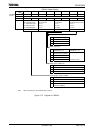
Internal data bus
TA01RUN<TA0RDE>
Timer register A0 (TA0REG)
Register buffer 0
Shift trigger
B
Selector
SA
Write
Write to TA0REG
Match detecting PPG cycle
PWM 2
n
overflow