


TMP92CM22
2007-02-16
92CM22-82
(2) Connection memory specification
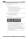
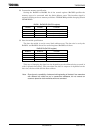
Setting the BnOM1 to BnOM0 bit of the control register (BnCSH) specifies the
memory type to be connected with the block address areas. The interface signal is
output according to the set memory as follows. TMP92CM22 prohibit changing default
(SRAM/ROM).
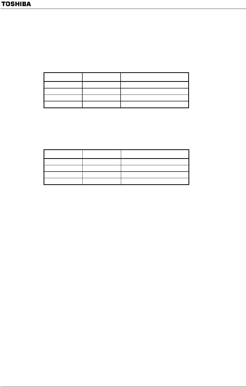
BnOM1, BnOM0 Bit (BnCSH register)
BnOM1 BnOM0 Function
0 0 SRAM/ROM (Default)
0 1 (Reserved)
1 0 (Reserved)
1 1 (Reserved)
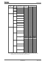
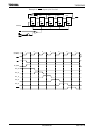
(3) Data bus width specification
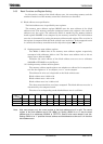
The data bus width is set for every block address area. The bus size is set by the
BnBUS1 and BnBUS0 bits of the control register (BnCSH) as follows.
BnBUS Bit (BnCSH register)
BnBUS1 BnBUS0 Function
0 0 8-bit bus mode (Default)
0 1 16-bit bus mode
1 0 (Reserved)
1 1 (Reserved)
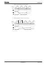
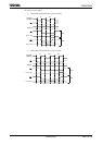
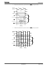
This way of changing the data bus size depending on the address being accessed is
called “dynamic bus sizing”. The part where the data is output to is depended on the
data size, the bus width and the start address.
Note: Since there is a possibility of abnormal writing/reading of the data if two memories
with different bus width are put in consecutive addresses, do not execute an
access to placed on both memories with one command.