


TMP92CM22
2007-02-16
92CM22-251
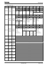
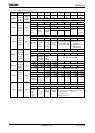
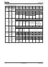
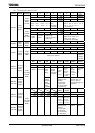
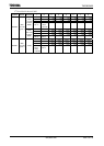
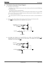
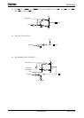
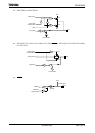
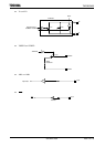
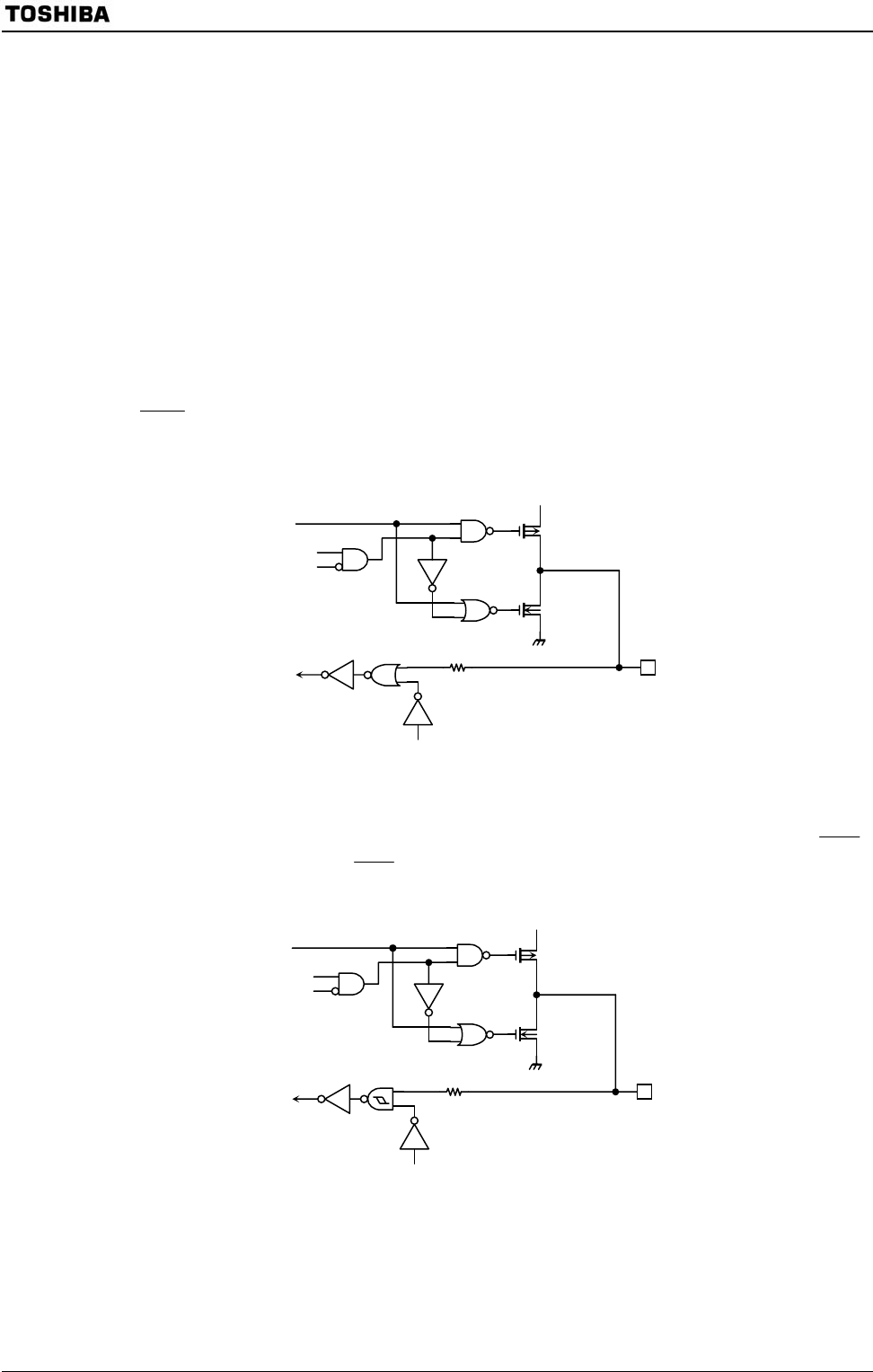
6. Port Section Equivalent Circuit Diagram
■ Reading the circuit diagram
Basically, the gate symbols written are the same as those used for the standard CMOS logic
IC [74HCXX] series.
The dedicated signal is described below.
STOP: This signal becomes active “1” when the halt mode setting register is set to the STOP
mode and the CPU executes the HALT instruction. When the drive enable bit <DRVE> is set
to “1”, however, STOP remains at “0”.
The input protection resistance ranges from several tens of ohms to several hundreds of
ohms.
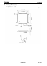
■ Data bus (D0 to D7), P1 (D8 to D15), P4 (A0 to A7), P5 (A8 to A15), P6 (A16 to A23),
P76 (
WAIT ), PD2 (TB1OUT0), PD3 (TB1OUT1), PF6, and PF7
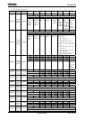
■ P90 (SCK), PC0 (TA0IN), PC1 (TA1OUT/INT1), PC3 (INT0), PC5 (TA3OUT/INT2), PC6
(TB0OUT/INT3), PD0 (INT4/TB1IN0), PD1 (INT5/TB1IN1), PF1 (RXD0), PF2 (SCLK0/
CTS0 ),
PF4 (RXD1), and PF5 (SCLK1/
CTS1 )
VCC
O
utput
d
ata
O
utput ena
bl
e
Stop
I
nput
d
ata
I/O
I
nput ena
bl
e
P-ch
N
-c
h
VCC
O
utput
d
ata
O
utput ena
bl
e
Stop
I
nput
d
ata
I/O
I
nput
enable
P-ch
N-ch