


TMP92CM22
2007-02-16
92CM22-13
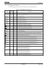
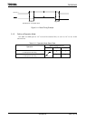
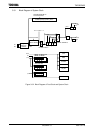
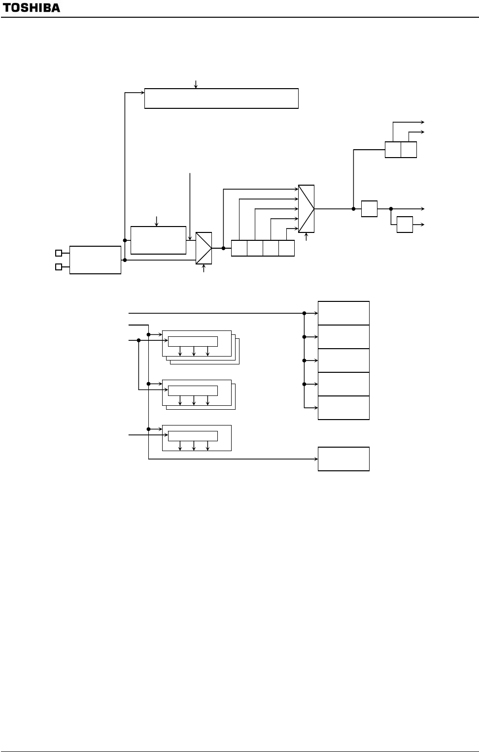
3.3.1 Block Diagram of System Clock
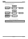
Figure 3.3.2 Block Diagram of Dual Clock and System Clock
÷4
÷16÷8÷4÷2
X2
fc/16
fc/8
fc/4
fc/2
÷8
φT
φT0
f
FPH
÷2
÷2
f
SYS
f
iO
fc
PLLCR<FCSEL>
Clock gear
High-
frequency
oscillator
X1
PLLCR<PLLON>
Warm-up timer (for high-frequency
oscillator)/lockup (for PLL) timer
SYSCR1<GEAR2:0>
f
OSCH
SYSCR2<WUPTM1:0>
PLLCR<PLUPFG>
CPU
RAM
Interrupt
controller
ADC
I/O port
WDT
f
SYS
f
iO
Prescaler
SIO0 and SIO1
Prescaler
φT0
f
PLL
= f
OSCH
×
4
SBI
Prescaler
φT
TMRA0 to TMRA3 and
TMRB0 to TMRB1
PLL
(Clock doubler)