


TMP92CM22
2007-02-16
92CM22-61
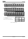
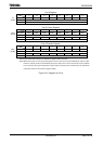
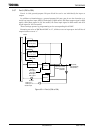
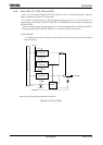
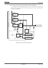
Figure 3.5.10 Port 7 (P76)
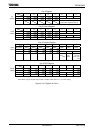
Port 7 Register
7 6 5 4 3 2 1 0
Bit symbol P76 P75 P74 P73 P72 P71 P70
Read/Write R/W
After reset Data from
external
port (Note)
1 1 1 1 1 1
Note: Output latch register is cleared to 0.
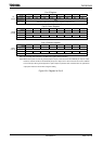
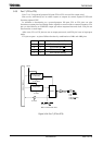
Port 7 Control Register
7 6 5 4 3 2 1 0
Bit symbol P76C
Read/Write W
After reset 0
Function
0: Input
1: Output
Port 7 Function Register
7 6 5 4 3 2 1 0
Bit symbol P76F P75F P74F P73F P72F P71F P70F
Read/Write W
After reset 0 0 0 0 0 0 1
Function 0: Port
1:
WAIT
0: Port
1: R/ W
0: Port
1: CLKOUT
0: Port
1:
Don’t set
0: Port
1:
WRLU
0: Port
1:
WRLL
0: Port
1: RD
Note: Read-modify-write instruction is prohibited for registers P7CR and P7FC.
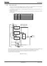
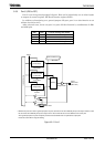
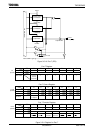
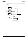
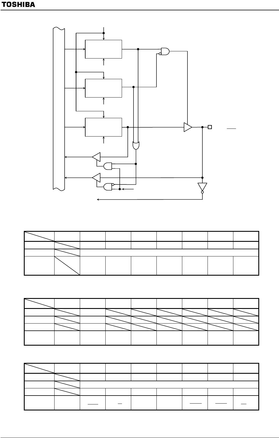
Figure 3.5.11 Register for Port 7
P7FC
(001FH)
P7
(001CH)
P7CR
(001EH)
Internal data bus
Direction control
(on bit basis)
Reset
P7CR write
S
Output latch
P7 write
P7 read
Port P7
P76 (
WAIT
)
Function control
(on bit basis)
P7FC write
Output buffer
Internal WAIT signal