


TMP92CM22
2007-02-16
92CM22-118
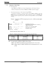
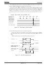
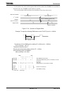
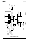
In this mode, the value of the register buffer will be shifted into TA0REG if 2
n
overflow is
detected when the TA0REG double buffer is enabled.
Use of the double buffer facilitates the handling of low duty ratio waves.
Figure 3.7.18 Operation of Register Buffer
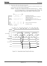
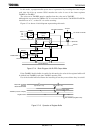
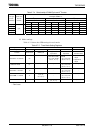
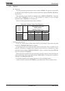
Example: To output the following PWM waves on the TA1OUT pin at f
C
= 40 MHz:
To achieve a 51.2 μs PWM cycle by setting φT1=(16/fc)s (at f
C
= 40 MHz):
51.2 μs/(16/fc)s = 128 = 2
n
Therefore n should be set to 7.
Since the low-level period is 36.0 μs when φT1 = (16/fc)s,
set the following value for TA0REG:
36.0 μs/(16/fc)s = 90 = 5AH
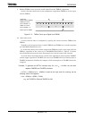
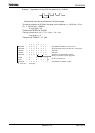
MSB LSB
7 6 5 4 3210
TA01RUN ←
− X X X
− − −
0 Stop TMRA0 and clear it to 0.
TA01MOD ← 1 1 1 0
− −
0 1 Select 8-bit PWM mode (cycle: 2
7
) and select φT1 as the
input clock.
TA0REG ← 0 1 0 1 1010 Write 5AH.
TA1FFCR ← X X X X 101X Clear TA1FF to 0; set inversion to enable.
PCCR ← X
− −
X − X1−
PCFC ←
X
− −
X
−
X1−
Set PC1 to TA1OUT pin.
TA01RUN ←
1 X X X
−
1 − 1 Start TMRA0 counting.
X : Don’t care, − : No change
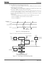
Q
2
Q
1
Match with TA0REG
Q
3
Q
2
Up counter
=
Q
1
Up counter = Q
2
Shift from TA0REG (Register buffer)
Write to TA0REG
TA0REG
(Value of compare)
Re
g
ister buffe
r
2
n
overflow
36.0
μ
s
51.2
μ
s