


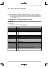
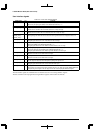
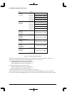
II CORE BLOCK: BCU (Bus Control Unit)
B-II-4-6 EPSON S1C33210 FUNCTION PART
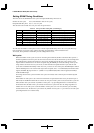
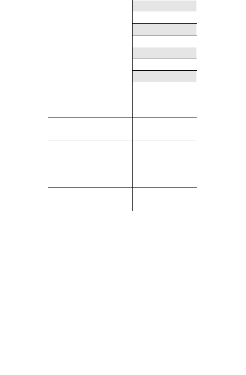
Area
Area 17+18 (#CE17+18)
SRAM type
8 or 16 bits
Areas 15–16 (#CE15+16)
SRAM type
8 or 16 bits
Area 14 (#CE14/#RAS3)
SRAM type
DRAM type
8 or 16 bits
Area 13 (#CE13/#RAS2)
SRAM type
DRAM type
8 or 16 bits
Areas 11–12 (#CE11+12)
SRAM type
8 or 16 bits
Areas 9–10 (#CE9+10EX)
SRAM type
Burst ROM type
8 or 16 bits
Areas 7–8 (#CE7+8)
SRAM type
8 or 16 bits
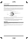
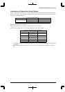
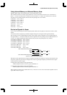
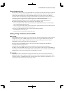
0xFFFFFFF
0xD000000
0xCFFFFFF
0xC000000
0xBFFFFFF
0x9000000
0x8FFFFFF
0x8000000
0x7FFFFFF
0x7000000
0x6FFFFFF
0x6000000
0x5FFFFFF
0x5000000
0x4FFFFFF
0x4000000
0x3FFFFFF
0x3000000
0x2FFFFFF
0x2000000
0x1FFFFFF
0x1000000
0x0FFFFFF
0x0800000
0x07FFFFF
0x0400000
Address
External memory 4 (16MB)
External memory 5 (16MB)
External memory 2 (8MB)
External memory 3 (16MB)
External memory 1 (4MB)
CEFUNC = "10" or "11"
External memory 7 (16MB)
External memory 7' (16MB)
(Mirror of External memory 7')
(Mirror of External memory 7)
External memory 6 (16MB)
External memory 6' (16MB)
(Mirror of External memory 6')
(Mirror of External memory 6)
Figure 4.2 External System Memory Map
Furthermore, the #CE4+#CE5 and #CE6 signals can be output from the P30 and P34 terminals, respectively.
This function expands the accessible area when CEFUNC is set to "01, "10" or "11".
To output the #CE4+#CE5 signal from the P30 terminal:
CFP30 (D0)/P3 function select register (0x402DC) = "1"
IOC30 (D0)/P3 I/O control register (0x402DE) = "1"
To output the #CE6 signal from the P34 terminal:
CFP34 (D4)/P3 function select register (0x402DC) = "1"
IOC34 (D4)/P3 I/O control register (0x402DE) = "1"
The P30 and P34 terminals are set for the general I/O ports at initial reset.
The P30 and P34 terminals are shared with the #WAIT input and the #BUSREQ input, respectively. Therefore,
when using the #WAIT and #BUSREQ signals, these terminals cannot be used for #CE4+#CE5 and #CE6 outputs.