


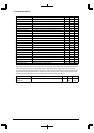
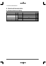
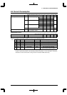
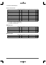
8 ELECTRICAL CHARACTERISTICS
A-72 EPSON S1C33210 PRODUCT PART
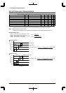
8.5 A/D Converter Characteristics
(Unless otherwise specified: AVDD=VDD=2.7V to 3.6V, VSS=0V, Ta=-40°C to +85°C, ST[1:0]=11)
Item Symbol Condition Min. Typ. Max. Unit ∗
Resolution – – 10 – bit
Conversion time – 10 – 625 µs1
Zero scale error EZS 024LSB
Full scale error EFS -2 – 2 LSB
Integral linearity error EL -3 – 3 LSB
Differential linearity error ED -3 – 3 LSB
Permissible signal source impedance – – – 5 kΩ
Analog input capacitance – – – 45 pF
∗ note 1) Indicates the minimum value when A/D clock = 2MHz (maximum clock frequency in 3V system).
Indicates the maximum value when A/D clock = 32 kHz (minimum clock frequency in 3V system).
Note: • Be sure to use as VDD = AVDD.
• The A/D converter cannot be used when the S1C33210 is used with a 2V power source.
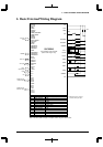
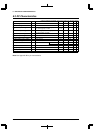
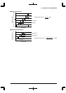
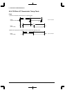
A/D conversion error
V[000]h = Ideal voltage at zero-scale point (=0.5LSB)
V'[000]h = Actual voltage at zero-scale point
V[3FF]h = Ideal voltage at full-scale point (=1022.5LSB)
V'[3FF]h = Actual voltage at full-scale point
1LSB =
1LSB' =
AV
DD
- V
SS
2
10
- 1
V'[3FF]h - V'[000]h
2
10
- 2
V[000]h
(=0.5LSB)
V'[000]h
004
003
002
001
000
V
SS
Zero scale error
Zero scale error E
ZS
= [LSB]
(V'[000]h - 0.5LSB') - (V[000]h - 0.5LSB)
1LSB
Digital output (hex)
Analog input
Ideal conversion characteristic
Actual conversion characteristic
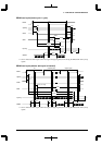
V[3FF]h (=1022.5LSB)
V'[3FF]h
3FF
3FE
3FD
3FC
3FB
AV
DD
Full scale error
Full scale error E
FS
= [LSB]
(V'[3FF]h + 0.5LSB') - (V[3FF]h + 0.5LSB)
1LSB
Digital output (hex)
Analo
g
input
Ideal conversion characteristic
Actual conversion characteristic