


4 PERIPHERAL CIRCUITS
A-40 EPSON S1C33210 PRODUCT PART
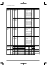
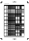
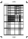
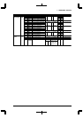
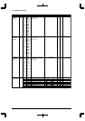
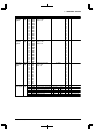
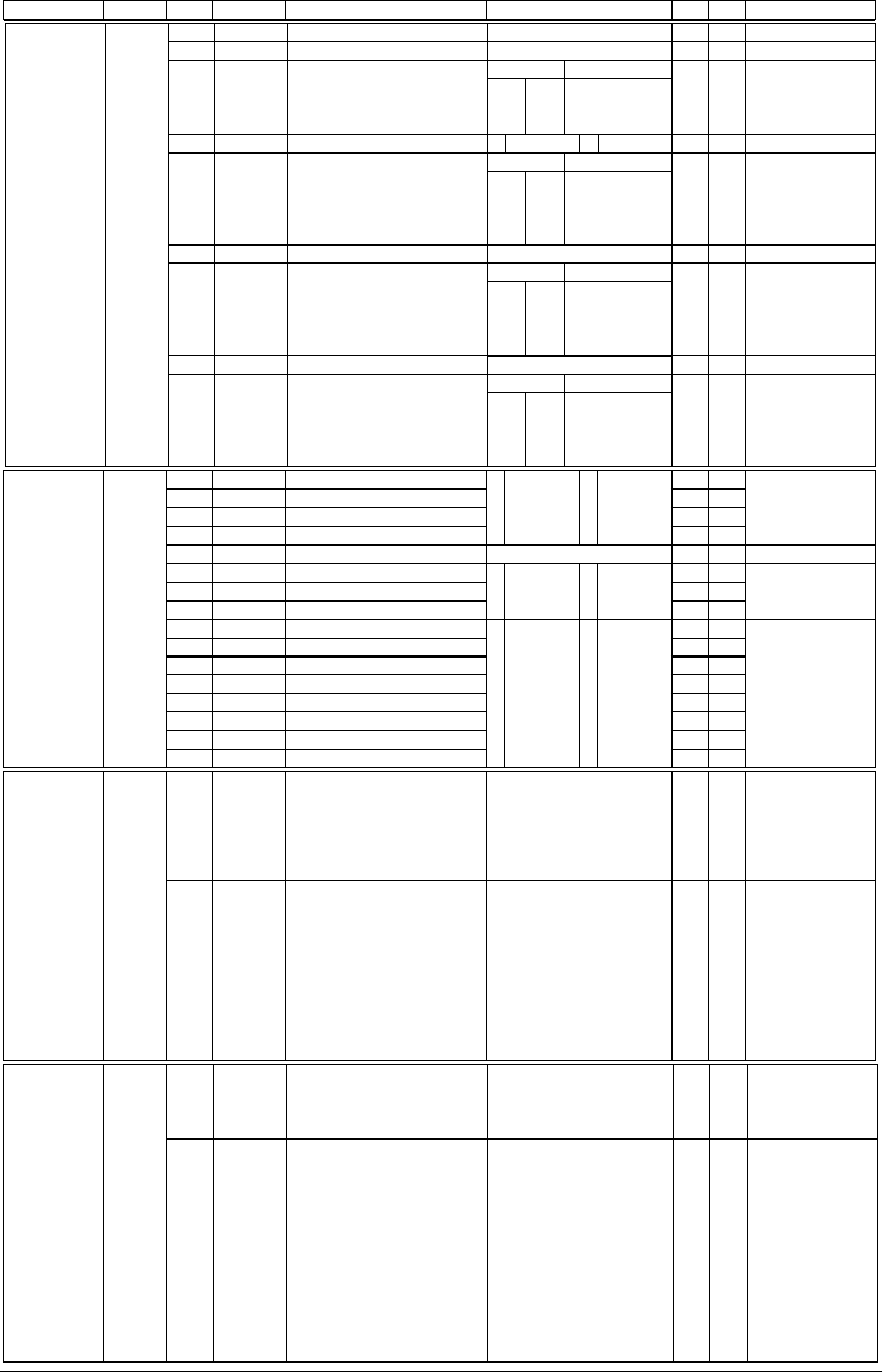
NameAddressRegister name Bit Function Setting Init. R/W Remarks
1 Successive 0 Normal
–
–
CEFUNC1
CEFUNC0
CRAS
RPRC1
RPRC0
–
CASC1
CASC0
–
RASC1
RASC0
DF–C
DB
DA
D9
D8
D7
D6
D5
D4
D3
D2
D1
D0
reserved
reserved
#CE pin function selection
Successive RAS mode setup
DRAM
RAS precharge cycles selection
reserved
DRAM
CAS cycles selection
reserved
DRAM
RAS cycles selection
– –
–
0
0
0
0
0
–
0
0
–
0
0
–
–
R/W
R/W
R/W
–
R/W
–
R/W
0 when being read.
Undefined when read.
0 when being read.
0 when being read.
0048130
(HW)
1
0
0
x
1
0
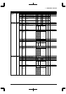
CFFUNC[1:0]
#CE output
#CE7/8..#CE17/18
#CE6..#CE17
#CE4..#CE10
1
1
0
0
1
0
1
0
RPRC[1:0] Number of cycles
4
3
2
1
–
1
1
0
0
1
0
1
0
CASC[1:0] Number of cycles
4
3
2
1
–
1
1
0
0
1
0
1
0
RASC[1:0] Number of cycles
4
3
2
1
DRAM timing
set-up register
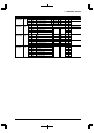
–
–
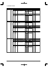
1 Internal
access
0 External
access
1 Internal
access
0 External
access
1 Big endian 0
Little endian
A18IO
A16IO
A14IO
A12IO
–
A8IO
A6IO
A5IO
A18EC
A16EC
A14EC
A12EC
A10EC
A8EC
A6EC
A5EC
DF
DE
DD
DC
DB
DA
D9
D8
D7
D6
D5
D4
D3
D2
D1
D0
Area 18, 17 internal/external access
Area 16, 15 internal/external access
Area 14, 13 internal/external access
Area 12, 11 internal/external access
reserved
Area 8, 7 internal/external
access
Area 6 internal/external
access
Area 5, 4 internal/external
access
Area 18, 17 endian control
Area 16, 15 endian control
Area 14, 13 endian control
Area 12, 11 endian control
Area 10, 9 endian control
Area 8, 7 endian control
Area 6 endian control
Area 5, 4 endian control
0
0
0
0
0
0
0
0
0
0
0
0
0
0
0
0
R/W
R/W
R/W
R/W
–
R/W
R/W
R/W
R/W
R/W
R/W
R/W
R/W
R/W
R/W
R/W
0 when being read.
0048132
(HW)
Access control
register
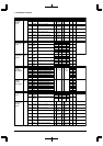
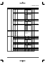
TTBR15
TTBR14
TTBR13
TTBR12
TTBR11
TTBR10
TTBR09
TTBR08
TTBR07
TTBR06
TTBR05
TTBR04
TTBR03
TTBR02
TTBR01
TTBR00
DF
DE
DD
DC
DB
DA
D9
D8
D7
D6
D5
D4
D3
D2
D1
D0
Trap table base address [15:10]
Trap table base address [9:0]
Fixed at 0
0
0
0
0
0
0
0
0
0
0
0
0
0
0
0
0
R/W
R
0 when being read.
Writing 1 not allowed.
0048134
(HW)
TTBR low-
order register
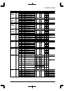
TTBR33
TTBR32
TTBR31
TTBR30
TTBR2B
TTBR2A
TTBR29
TTBR28
TTBR27
TTBR26
TTBR25
TTBR24
TTBR23
TTBR22
TTBR21
TTBR20
DF
DE
DD
DC
DB
DA
D9
D8
D7
D6
D5
D4
D3
D2
D1
D0
Trap table base address [31:28]
Trap table base address [27:16]
Fixed at 0
0x0C0
0
0
0
0
0
0
0
0
1
1
0
0
0
0
0
0
R
R/W
0 when being read.
Writing 1 not allowed.
0048136
(HW)
TTBR high-
order register