


4 PERIPHERAL CIRCUITS
S1C33210 PRODUCT PART EPSON A-39
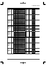
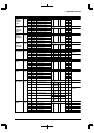
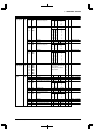
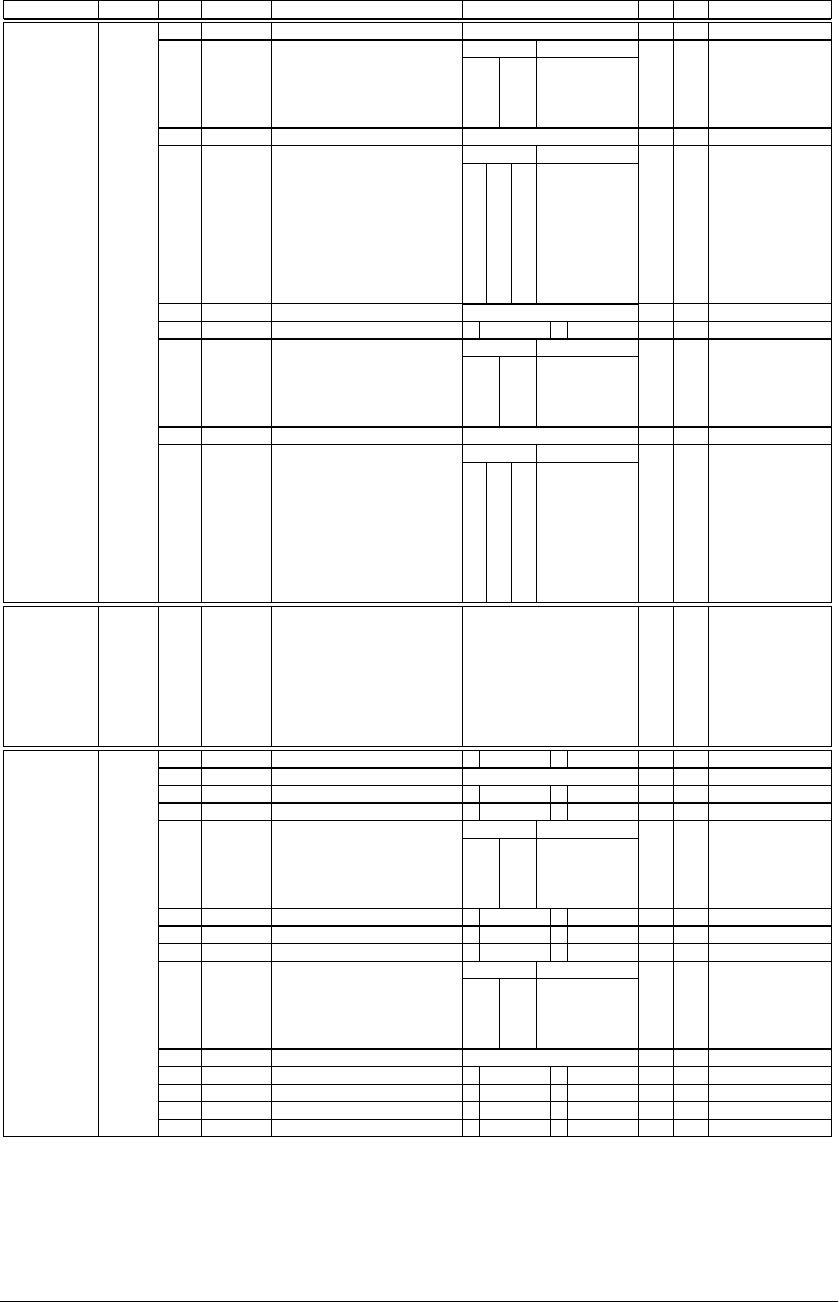
NameAddressRegister name Bit Function Setting Init. R/W Remarks
–
A6DF1
A6DF0
–
A6WT2
A6WT1
A6WT0
–
A5SZ
A5DF1
A5DF0
–
A5WT2
A5WT1
A5WT0
DF–E
DD
DC
DB
DA
D9
D8
D7
D6
D5
D4
D3
D2
D1
D0
reserved
Area 6
output disable delay time
reserved
Area 6 wait control
reserved
Areas 5–4 device size selection
Areas 5–4
output disable delay time
reserved
Areas 5–4 wait control
–
–
–
1 8 bits 0 16 bits
–
1
1
–
1
1
1
–
0
1
1
–
1
1
1
–
R/W
–
R/W
–
R/W
R/W
–
R/W
0 when being read.
0 when being read.
0 when being read.
0 when being read.
004812A
(HW)
Areas 6–4
set-up register
1
1
0
0
1
0
1
0
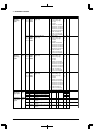
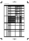
A6DF[1:0] Number of cycles
3.5
2.5
1.5
0.5
1
1
0
0
1
0
1
0
A5DF[1:0] Number of cycles
3.5
2.5
1.5
0.5
1
1
1
1
0
0
0
0
1
1
0
0
1
1
0
0
1
0
1
0
1
0
1
0
A6WT[2:0] Wait cycles
7
6
5
4
3
2
1
0
1
1
1
1
0
0
0
0
1
1
0
0
1
1
0
0
1
0
1
0
1
0
1
0
A5WT[2:0] Wait cycles
7
6
5
4
3
2
1
0
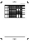
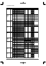
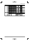
TBRP7
TBRP6
TBRP5
TBRP4
TBRP3
TBRP2
TBRP1
TBRP0
D7
D6
D5
D4
D3
D2
D1
D0
TTBR register write protect 0
0
0
0
0
0
0
0
W Undefined in read.004812D
(B)
Writing 01011001(0x59)
removes the TTBR (0x48134)
write protection.
Writing other data sets the
write protection.
TTBR write
protect register
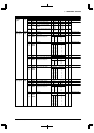
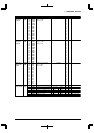
RBCLK
–
RBST8
REDO
RCA1
RCA0
RPC2
RPC1
RPC0
RRA1
RRA0
–
SBUSST
SEMAS
SEPD
SWAITE
DF
DE
DD
DC
DB
DA
D9
D8
D7
D6
D5
D4
D3
D2
D1
D0
BCLK output control
reserved
Burst ROM burst mode selection
DRAM page mode selection
Column address size selection
Refresh enable
Refresh method selection
Refresh RPC delay setup
Refresh RAS pulse width
selection
reserved
External interface method selection
External bus master setup
External power-down control
#WAIT enable
–
–
1 Fixed at H 0 Enabled
1
8-successive
0
4-successive
1 Enabled 0 Disabled
1 Self-refresh 0
CBR-refresh
1 2.0 0 1.0
1 #BSL 0 A0
1 Existing 0 Nonexistent
1 Enabled 0 Disabled
1 Enabled 0 Disabled
1 EDO 0 Fast page
0
0
0
0
0
0
0
0
0
0
0
0
0
0
0
0
R/W
–
R/W
R/W
R/W
R/W
R/W
R/W
R/W
–
R/W
R/W
R/W
R/W
Writing 1 not allowed.
Writing 1 not allowed.
004812E
(HW)
1
1
0
0
1
0
1
0
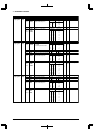
RCA[1:0] Size
11
10
9
8
1
1
0
0
1
0
1
0
RRA[1:0] Number of cycles
5
4
3
2
Bus control
register