


III PERIPHERAL BLOCK: SERIAL INTERFACE
S1C33210 FUNCTION PART EPSON B-III-8-39
SSCK0: Ch.0 input clock selection (D2) / Serial I/F Ch.0 control register (0x401E3)
SSCK1: Ch.1 input clock selection (D2) / Serial I/F Ch.1 control register (0x401E8)
SSCK2: Ch.2 input clock selection (D2) / Serial I/F Ch.2 control register (0x401F3)
SSCK3: Ch.3 input clock selection (D2) / Serial I/F Ch.3 control register (0x401F8)
Selects the clock source for an asynchronous transfer.
Write "1": #SCLK (external clock)
Write "0": Internal clock
Read: Valid
During operation in the asynchronous mode, this bit is used to select the clock source between an internal clock
(output by an 8-bit programmable timer) and an external clock (input from the #SCLKx pin). An external clock is
selected by writing "1" to this bit, and an internal clock is selected by writing "0".
At initial reset, SSCKx becomes indeterminate.
SMD01–SMD00: Ch.0 transfer mode selection (D[1:0]) / Serial I/F Ch.0 control register (0x401E3)
SMD11–SMD10: Ch.1 transfer mode selection (D[1:0]) / Serial I/F Ch.1 control register (0x401E8)
SMD21–SMD20: Ch.2 transfer mode selection (D[1:0]) / Serial I/F Ch.2 control register (0x401F3)
SMD31–SMD30: Ch.3 transfer mode selection (D[1:0]) / Serial I/F Ch.3 control register (0x401F8)
Sets the transfer mode of the serial interface as shown in Table 8.15 below.
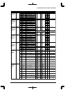
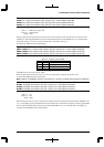
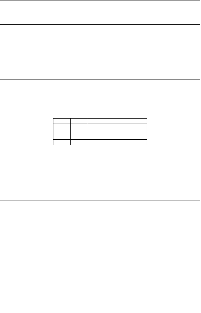
Table 8.15 Setting of Transfer Mode
SMDx1 SMDx0 Transfer mode
1 1 8-bit asynchronous mode
1 0 7-bit asynchronous mode
0 1 Clock-synchronized slave mode
0 0 Clock-synchronized master mode
The SMDx bit can be read as well as written.
When using the IrDA interface, always be sure to set an asynchronous mode for the transfer mode.
At initial reset, SMDx becomes indeterminate.
Note: SSCK11 and SSCK31 must be "0" because Ch. 1 and Ch. 3 support only asynchronous operation.
DIVMD0: Sampling clock division ratio (D4) / Serial I/F Ch.0 IrDA register (0x401E4)
DIVMD1: Sampling clock division ratio (D4) / Serial I/F Ch.1 IrDA register (0x401E9)
DIVMD2: Sampling clock division ratio (D4) / Serial I/F Ch.2 IrDA register (0x401F4)
DIVMD3: Sampling clock division ratio (D4) / Serial I/F Ch.3 IrDA register (0x401F9)
Selects the division ratio of the sampling clock.
Write "1": 1/8
Write "0": 1/16
Read: Valid
Select the division ratio necessary to generate the sampling clock for asynchronous transfers. When DIVMDx is set
to "1", the sampling clock is generated from the input clock of the serial interface (output by an 8-bit programmable
timer or input from #SCLKx) by dividing it by 8. When DIVMDx is set to "0", the input clock is divided by 16.
At initial reset, DIVMDx becomes indeterminate.