


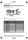
III PERIPHERAL BLOCK: INPUT/OUTPUT PORTS
B-III-9-8 EPSON S1C33210 FUNCTION PART
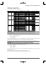
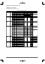
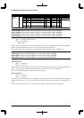
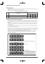
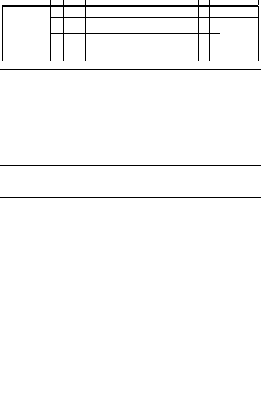
NameAddressRegister name Bit Function Setting Init. R/W Remarks
–
CFEX5
CFEX4
CFEX3
CFEX2
CFEX1
CFEX0
D7-6
D5
D4
D3
D2
D1
D0
reserved
P05 port extended function
P04 port extended function
P31 port extended function
P21 port extended function
P10, P11, P13 port extended
function
P12, P14 port extended function
–
0
0
0
0
1
1
–
R/W
R/W
R/W
R/W
R/W
R/W
Undefined when read.
Always set to 0.
Always set to 0.
00402DF
(B)
Port function
extension
register
1
1
–
0 P05, etc.
1
–
0 P04, etc.
1 #GARD 0 P31, etc.
1 #GAAS 0 P21, etc.
1 DST0
DST1
DPC0
0 P10, etc.
P11, etc.
P13, etc.
1 DST2
DCLK
0 P12, etc.
P14, etc.
–
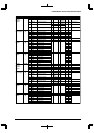
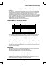
CFP05–CFP00: P0[5:0] function selection (D[5:0]) / P0 function select register (0x402D0)
CFP16–CFP10: P1[6:0] function selection (D[6:0]) / P1 function select register (0x402D4)
CFP27–CFP20: P2[7:0] function selection (D[7:0]) / P2 function select register (0x402D8)
CFP35–CFP30: P3[5:0] function selection (D[5:0]) / P3 function select register (0x402DC)
Selects the function of each I/O port pin.
Write "1": Used for peripheral circuit
Write "0": I/O port pin
Read: Valid
When a bit of the CFP register is set to "1", the corresponding pin is set for use with peripheral circuits (see Table 9.3).
The pins for which register bits are set to "0" can be used as general-purpose I/O ports.
At cold start, CFP is set to "0" (I/O port). At hot start, CFP retains its state from prior to the initial reset.
P05D–P00D: P0[5:0] I/O port data (D[5:0]) / P0 I/O port data register (0x402D1)
P16D–P10D: P1[6:0] I/O port data (D[6:0]) / P1 I/O port data register (0x402D5)
P27D–P20D: P2[7:0] I/O port data (D[7:0]) / P2 I/O port data register (0x402D9)
P35D–P30D: P3[5:0] I/O port data (D[5:0]) / P3 I/O port data register (0x402DD)
This register reads data from I/O-port pins or sets output data.
When writing data
Write "1": High level
Write "0": Low level
When an I/O port is set for output, the data written to it is directly output to the I/O port pin. If the data written to the
port is "1", the port pin is set high (V
DD level); if the data is "0", the port pin is set low (VSS level).
Even in the input mode, data can be written to the port data register.
When reading data
Read "1": High level
Read "0": Low level
The voltage level on the port pin is read out regardless of whether an I/O port is set for input or output mode. If the pin
voltage is high (V
DD level), "1" is read out as input data; if the pin voltage is low (VSS level), "0" is read out as input
data.
At cold start, all data bits are set to "0". At hot start, they retain their state from prior to the initial reset.