


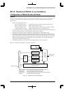

III PERIPHERAL BLOCK: MONITORED MOBILE ACCESS INTERFACES
B-III-10-2 EPSON S1C33210 FUNCTION PART
I/O Pins for Mobile Access Interfaces
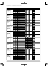
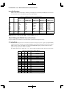
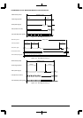
Table 10.1 lists the I/O pins for the mobile access interfaces.
Table 10.1 I/O Pins for Mobile Access Interfaces
Pin Name I/O Function Function Selection Bit
DTR O DTR output MSEL pin input is at High level *
1
RTS O RTS output MSEL pin input is at High level *
1
TXD O TXD output MSEL pin input is at High level *
1
RI I RI input MSEL pin input is at High level *
1
CTS I CTS input MSEL pin input is at High level *
1
DCD I DCD input MSEL pin input is at High level *
1
DSR I DSR input MSEL pin input is at High level *
1
RXD I RXD input MSEL pin input is at High level *
1
CNT1 O Mobile access control output #1
CNT2 O Mobile access control output #2
MSEL I Serial IF Ch. 3 configuration input. Normally
drive this at High level.
GOUT O NMI interrupt request output
*1: The communications macro select (MCRS) register (D[1:0]/0x200000) configures the I/O signals to match the
target mobile device.
MSEL (Serial IF interface Ch. 3 configuration input)
This pin specifies the operation of the serial IF Ch. 3 data I/O (SIN3 and SOUT3).
Low level input directly connects the RXD input pin to the SIN3 input and the TXD output pin to the SOUT3
output for asynchronous operation via the RXD and TXD pins.
High level input configures SIN3 and SOUT3 as necessary for UART, HDLC, PDC and PHS operation with
the mobile device.
RXD (RXD input pin)
This input pin accepts serial data from the mobile device.
UART communications feeds asynchronous serial data to the serial IF Ch. 3.
HDLC communications feeds clock-synchronous serial data to the packet processor block.
PDC communications feeds PDC signal receive data to the PDC processor block.
PHS communications feeds PHS signal receive data to the PIAFS processor block.
TXD (TXD output pin)
This output pin feeds serial data to the mobile device.
UART communications feeds asynchronous serial data from the serial IF Ch. 3.
HDLC communications feeds clock-synchronous serial data from the packet processor block.
PDC communications feeds PDC signal receive data from the PDC processor block.
PHS communications feeds PHS signal receive data from the PIAFS processor block.
DCD (DCD input pin)
The function of this input pin depends on the communications mode.
UART communications interprets this input as the DCD signal from the mobile device. A bit in the
communications block modem status register (0x020002A) tracks the input level.
HDLC communications does not assign any meaning to this input. A bit in the communications block modem
status register (0x020002A) tracks the input level.
PDC communications feeds this PDC frame synchronization signal to the PDC processor block. A bit in the
communications block modem status register (0x020002A) tracks the input level.
PHS communications feeds this PHS frame synchronization signal to the PIAFS processor block. A bit in the
communications block modem status register (0x020002A) tracks the input level.