


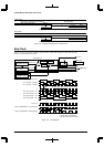

II CORE BLOCK: BCU (Bus Control Unit)
B-II-4-22 EPSON S1C33210 FUNCTION PART
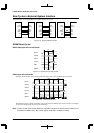
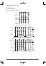
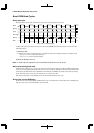
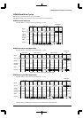
Burst ROM Read Cycles
Burst read cycle
Example: When 4-consecutive-burst and 2-wait cycles are set during the first access
BCLK
A[23:2]
A[1:0]
#CE10(9)
D[15:0]
#RD
addr[23:2]
"11""10""01""00"
IR3IR2IR1IR0
Figure 4.26 Burst Read Cycle
A burst read cycle occurs when area 10 or 9 is set for burst ROM and one of those areas is accessed for the
following reasons:
1) Instruction fetch
The burst read cycle is executed as long as a instruction fetch from contiguous addresses continues until
A[2:1] = "11" (for 4-consecutive bursts); or
A[3:1] = "111" (for 8-consecutive bursts)
2) Word (32-bit) data read out
Note: A 16-bit output is supported for the burst ROM. Set the device size to 16 bits.
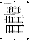
Wait cycles during burst read
In the first bus operation, 0 to 7 wait cycles can be inserted using the wait control bits A10WT[2:0] (D[2:0]) /
Areas 10–9 set-up register (0x48126) in the same way as for ordinary SRAM. For the wait cycles to be inserted
in the burst cycle that follows, use a dedicated wait control bits, A10BW[1:0], which is only used for reading
bursts. The wait cycles can be set in the range from 0 to 3 using these bits.
Note that no wait cycle via the #WAIT pin can be inserted into the burst-read cycle.
Write cycle to burst ROM area
If area 10 or 9 is set for burst ROM, a SRAM write cycle is executed when a write to that area is attempted. In
this case, wait cycles via the #WAIT pin can be inserted.