III PERIPHERAL BLOCK: LOW-SPEED (OSC1) OSCILLATION CIRCUIT
B-III-6-4 EPSON S1C33210 FUNCTION PART
Power-Control Register Protection Flag
The power-control register (SOSC1, SOSC3, CLKCHG, CLKDT[1:0]) at address 0x40180, which is used to
control the oscillation circuits and the CPU operating clock, is normally disabled against writing in order to prevent
it from malfunctioning due to unnecessary writing.
To enable this register for writing, the power-control register protection flag CLGP[7:0] (D[7:0]) / Power-control
protection register (0x4019E) must be set to "0b10010110". Note that this setting allows for the power-control
register (0x40180) to be written to only once, so all bits of CLGP[7:0] are cleared to "0" when this address is written
to. Therefore, CLGP[7:0] must be set to "0b10010110" each time the power-control register (0x40180) is written to.
The flag CLGP[7:0] does not affect the readout from the power-control register (0x40180).
Operation in Standby Mode
In HALT mode, which is entered by executing the halt instruction, the low-speed (OSC1) oscillation circuits retains
its status before HALT mode is entered. Under normal conditions, therefore, there is no need to control the
oscillation circuit before entering or after exiting HALT mode.
The low-speed (OSC1) oscillation circuit does not stop operating in SLEEP mode set by executing the slp (sleep)
instruction. Therefore, if the CPU was operating using the OSC1 clock before SLEEP mode was entered, the CPU
keeps operating using the OSC1 clock in SLEEP mode.
OSC1 Clock Output to External Devices
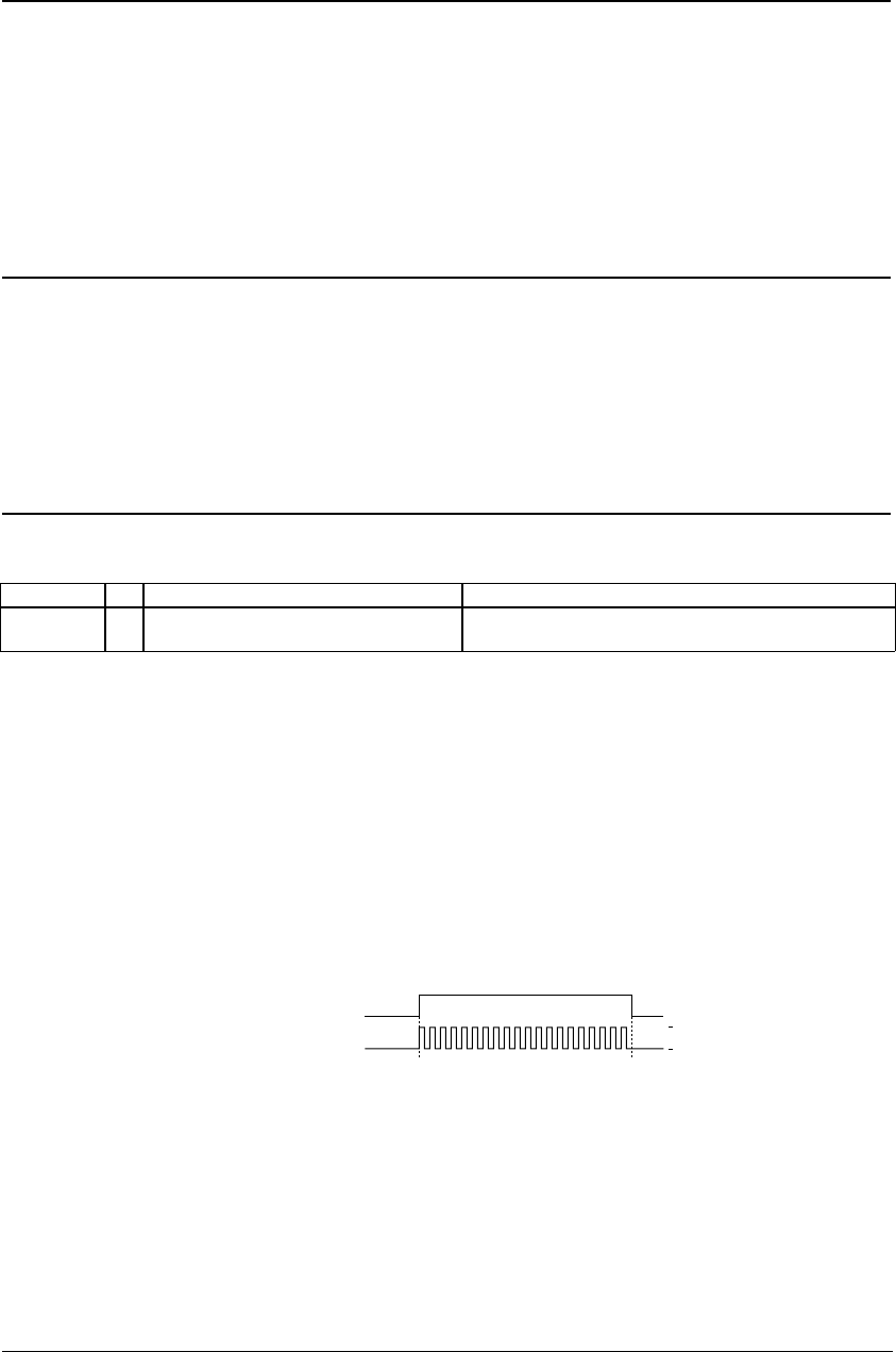
The low-speed (OSC1) oscillation clock can be output from the FOSC1 (P14) pin to external devices.
Table 6.2 OSC1 Clock Output Pin
Pin name I/O Function Function select bit
P14/FOSC1/
DCLK
I/O I/O port / Low-speed (OSC1) oscillation
clock output / DCLK signal output
CFP14(D4) / P1 function select register (0x402D4)
CFEX0 (D0) / Port function extension register (0x402DF)
Setting the clock output pin
The pin used to output the OSC1 clock to external devices is shared with the P14 I/O port and the debug clock
signal DCLK.
At cold start, it is set for the DCLK signal output (CFP14 = "0" and CFEX0 = "1"). When using the clock
output function, write "1" to CFP14 and "0" to CFEX0 (refer to "I/O Ports"), and also write "1" to IOC14
(0x402D6/D4).
At hot start, the pin retains its pre-reset status.
Output control
To start clock output, write "1" to PF1ON (D0) / Clock option register (0x40190). The clock output is stopped
by writing "0".
At initial reset, PF1ON is set to "0" (output disabled).
PF1ON register
FOSC1(P14) pin output
00
VDD
VSS
1
Figure 6.3 OSC1 Clock Output


