


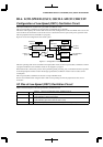
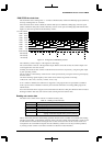

III PERIPHERAL BLOCK: LOW-SPEED (OSC1) OSCILLATION CIRCUIT
S1C33210 FUNCTION PART EPSON B-III-6-7
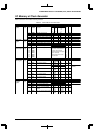
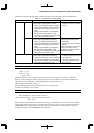
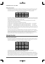
The following shows the operating status in HALT mode (basic mode and HALT2 mode) and SLEEP mode.
Table 6.4 Operating Status in Standby Mode
Standby mode Operating status Reactivating factor
HALT mode Basic mode • The CPU clock is stopped. (CPU stop status)
• BCU clock is supplied. (BCU run status)
• DMA clock is not stopped. (DMA run status)
• Clocks for the peripheral circuits maintain the
status before entering HALT mode. (run or
stop)
• The high-speed oscillation circuit maintains
the status before entering HALT mode.
• The low-speed oscillation circuit maintains the
status before entering HALT mode.
• Reset, NMI
• Enabled (not masked) interrupt
factors
HALT2 mode • The CPU clock is stopped. (CPU stop status)
• BCU clock is stopped. (BCU stop status)
• DMA clock is stopped. (DMA stop status)
• Clocks for the peripheral circuits maintain the
status before entering HALT mode. (run or
stop)
• The high-speed oscillation circuit maintains
the status before entering HALT mode.
• The low-speed oscillation circuit maintains the
status before entering HALT mode.
In HALT2 mode, operation can be
restarted by the following events.
• Reset, NMI
• The occurrence of an unmasked
interrupt
However, interrupts from peripheral
circuits require that the clock
supplied to the peripheral circuit in
question be operating.
SLEEP mode • The CPU clock is stopped. (CPU stop status)
• BCU clock is stopped. (BCU stop status)
• Clocks for the peripheral circuits are stopped.
• The high-speed oscillation circuit is stopped.
• The low-speed oscillation circuit maintains the
status before entering SLEEP mode.
• Reset, NMI
• Enabled (not masked) input port
interrupt factors
• Clock timer interrupt when the
low-speed oscillation circuit is
being operated
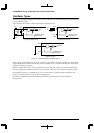
PF1ON: OSC1 external output control (D0) / Clock option register (0x40190)
Turns the low-speed (OSC1) clock output to external devices on or off.
Write "1": On
Write "0": Off
Read: Valid
The low-speed (OSC1) clock is output from the FOSC1 pin to an external device by writing "1" to PF1ON.
However, for this setting to be effective, the P14 pin must be set for the FOSC1 pin by CFP14 and CFEX0, and
output must be set by setting IOC14 (D4/0x402D6 <P1 I/O control register>) to "1".
The clock output is disabled by writing "0".
Writing to PF1ON is allowed only when CLGP[7:0] is set to "0b10010110".
At initial reset, PF1ON is set to "0" (Off).
CLGP7–CLGP0: Power-control register protection flag
([D[7:0]) / Power control protection register (0x4019E)
These bits remove the protection against writing to addresses 0x40180 and 0x40190.
Write "0b10010110": Write protection removed
Write other than the above: No operation (write-protected)
Read: Valid
Before writing to address 0x40180 or 0x40190, set CLGP[7:0] to "0b10010110" to remove the protection against
writing to that address. This clearing of write protection is effective for only one writing, so the bits are cleared to
"0b00000000" by one writing. Therefore, CLGP[7:0] must be set each time the protected address is written to.
At initial reset, CLGP is set to "0b00000000" (write-protected).