


II CORE BLOCK: BCU (Bus Control Unit)
B-II-4-18 EPSON S1C33210 FUNCTION PART
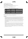
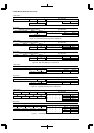
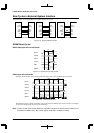
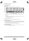
Bus Cycles in External System Interface
The following shows a sample SRAM connection the basic bus cycles.
A[9:1]
D[15:0]
#RD
#WRH
#WRL
#CE
S1C33
(1) A0 system (little endian/big endian)
A[8:0]
I/O[15:0]
#RD
#WRH
#WRL
#CE
SRAM
A[9:1]
D[15:0]
A0
#WRH
#WRL
#CE
#RD
S1C33
(2) #BSL system (little endian)
A[8:0]
I/O[15:0]
#LB
#UB
#WE
#OS
#OE
SRAM
A[9:1]
D[15:0]
A0
#WRH
#WRL
#CE
#RD
S1C33
(3) #BSL system (big endian)
A[8:0]
I/O[15:0]
#LB
#UB
#WE
#OS
#OE
SRAM
Figure 4.18 Sample DRAM Connection
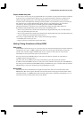
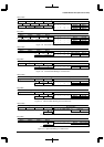
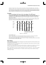
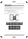
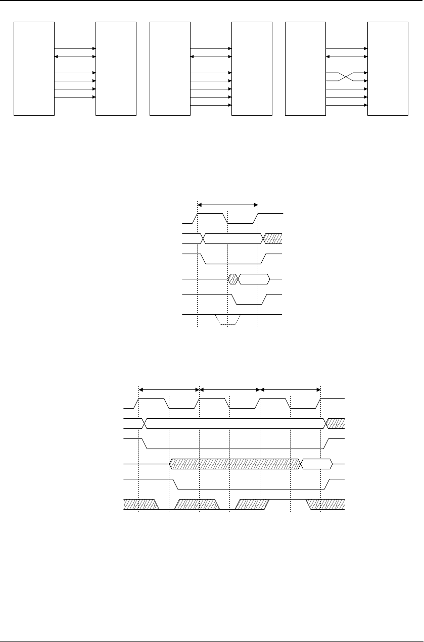
SRAM Read Cycles
Basic read cycle with no wait mode
BCLK
A[23:0]
#CExx
D[15:0]
#RD
#WAIT
addr
data
C1
Figure 4.19 Basic Read Cycle with No Wait
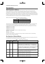
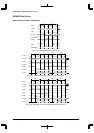
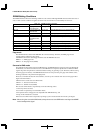
Read cycle with wait mode
Example: When the BCU has no internal wait mode and 2 wait cycles via #WAIT pin are inserted
BCLK
A[23:0]
#CExx
D[15:0]
#RD
#WAIT
C1 CW CW
addr
data
Figure 4.20 Read Cycle with Wait
The #WAIT signal is sampled at the falling edge of the transition of BCLK (bus clock) and when it is sampled
on an inactive (high level), the read cycle is terminated.
Note: Insertion of wait cycles via the #WAIT pin is possible only when the device for bus conditions is set
for SRAM, and SWAIT (D0) / Bus control register (0x4812E) is enabled for waiting.