


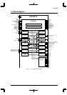

1 OUTLINE
A-10 EPSON S1C33210 PRODUCT PART
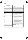
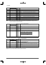
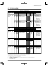
Pin name Pin No. I/O Pull-up Function
QFP15-128
DTR 95 O – DTR output *1
RTS 94 O – RTS output*1
TXD
SOUT3
100 O – TXD: TXD output*1 when MSEL pin input is at High level
SOUT3: SOUT3 output when MSEL pin input is at Low level
RI 97 I – RI input *1
CTS 101 I – CTS input *1
DCD 108 I – DCD input *1
DSR 96 I – DSR input *1
RXD
SIN3
107 I – RXD: RXD input when MSEL pin input is at High level
SIN3: SIN3 input when MSEL pin input is at Low level
CNT1 99 O – Mobile access control output #1
CNT2 98 O – Mobile access control output #2
MSEL 109 I Pull-up Serial I/O interface Ch. 3 configuration input. Normally drive this at High level.
GOUT 110 O – NMI interrupt request output
Note: *1 The communications macro select (MCRS) register (D[1:0]/0x200000) configures the I/O
signals to match the target mobile device.
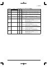
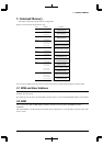
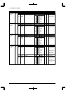
Table 1.3.5 List of Pins for Clock Generator
Pin name Pin No. I/O Pull-up Function
QFP15-128
OSC1 51 I – Low-speed (OSC1) oscillation input (32 kHz crystal oscillator or external clock
input)
OSC2 50 O – Low-speed (OSC1) oscillation output
OSC3 112 I – High-speed (OSC3) oscillation input (crystal/ceramic oscillator or external clock
input)
OSC4 113 O – High-speed (OSC3) oscillation output
PLLS[1:0] 105,106 I – PLL set-up pins
PLLS1 PLLS0 fin (fOSC3) fout (fPSCIN)
1110–25MHz 20–50MHz
0110–12.5MHz 40–50MHz
0 0 PLL is not
used
L
PLLC 103 ––Capasitor connecting pin for PLL
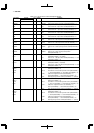
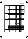
Table 1.3.6 List of Other Pins
Pin name Pin No. I/O Pull-up Function
QFP15-128 /down
TST 80 I Pull-
down
Test mode input. This pin is used for testing this chip. For further details, refer
to the S1C33 ASIC Design Guide.
DSIO 120 I/O Pull-up Serial I/O pin for debugging
This pin is used to communicate with the debugging tool S5U1C33000H.
#X2SPD 116 I – Clock doubling mode set-up pin1: CPU clock = bus clock × 1, 0: CPU clock = bus
clock × 2
#NMI 44 I Pull-up NMI request input pin
#RESET 43 I Pull-up Initial reset input pin
Note:"#" in the pin names indicates that the signal is low active.