


II CORE BLOCK: BCU (Bus Control Unit)
B-II-4-14 EPSON S1C33210 FUNCTION PART
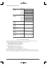
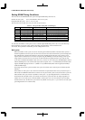
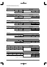
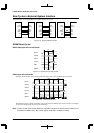
Byte 1
15 Data bus 0#WRL
1
#WRH
1
A0
0
A1
∗
No.
1
Byte 0
Bus operation
1
Sign or Zero extension Byte 1 Byte 0
31 0
Destination (general-purpose register)
A[1:0]=∗0
Source (16-bit device)
015
Little-endian
Byte 1
15 Data bus 0#WRL
1
#WRH
1
A0
0
A1
∗
No.
1 Byte 0
Bus operation
1
Sign or Zero extension Byte 1 Byte 0
31 0
Destination (general-purpose register)
A[1:0]=∗0
Source (16-bit device)
015
Big-endian
Figure 4.8 Half-word Data Reading from a 16-bit Device
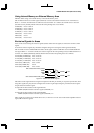
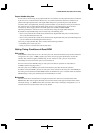
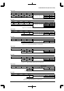
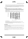
Byte 0
15
Data bus
0#WRL
1
0
#WRH
0
1
A0
1
0
A1
∗
∗
No.
1
1'
Data retained
Byte 0Data retained
Byte 3 Byte 2 Byte 1 Byte 0
31 0
A[1:0]=
∗
0A[1:0]=
∗
1
0
1'1
15
Source (general-purpose register)
Destination (16-bit device)
Bus operation
Little-endian
Byte 0
15
Data bus
0#WRL
1
0
#WRH
0
1
A0
0
1
A1
∗
∗
No.
1
1'
Data retained
Byte 0Data retained
Byte 3 Byte 2 Byte 1 Byte 0
31 0
A[1:0]=
∗
1A[1:0]=
∗
0
0
1'1
15
Source (general-purpose register)
Destination (16-bit device)
Bus operation
Big-endian
Figure 4.9 Byte Data Writing to a 16-bit Device
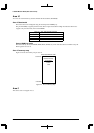
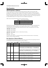
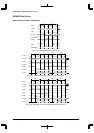
RD byte
15
Data bus
0#WRL
1
1
#WRH
1
1
A0
1
0
A1
∗
∗
No.
1
1'
Ignored
RD byteIgnored
RD byte
31 0
A[1:0]=
∗
0A[1:0]=
∗
1
0
1'1
15
Bus operation
Sign or Zero extension
Destination (general-purpose register)
Source (16-bit device)
Little-endian
RD byte
15
Data bus
0#WRL
1
1
#WRH
1
1
A0
0
1
A1
∗
∗
No.
1
1'
Ignored
RD byteIgnored
RD byte
31 0
A[1:0]=
∗
1A[1:0]=
∗
0
0
1'1
15
Bus operation
Sign or Zero extension
Destination (general-purpose register)
Source (16-bit device)
Big-endian
Figure 4.10 Byte Data Reading from a 16-bit Device
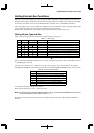
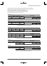
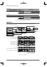
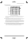
Data retained
15
Data bus
0#WRL
0
0
0
0
#WRH
X
X
X
X
A0
0
1
0
1
A1
0
0
1
1
No.
1
2
3
4
Byte 0
Data retained Byte 1
Data retained Byte 2
Data retained Byte 3
Byte 3 Byte 2 Byte 1 Byte 0
31 0
A[1:0]=10 A[1:0]=00A[1:0]=11 A[1:0]=01
80
14
888000
Source (general-purpose register)
Destination (8-bit device)
3 2
Bus operation
(X: Not connected/Unused)
Little-endian
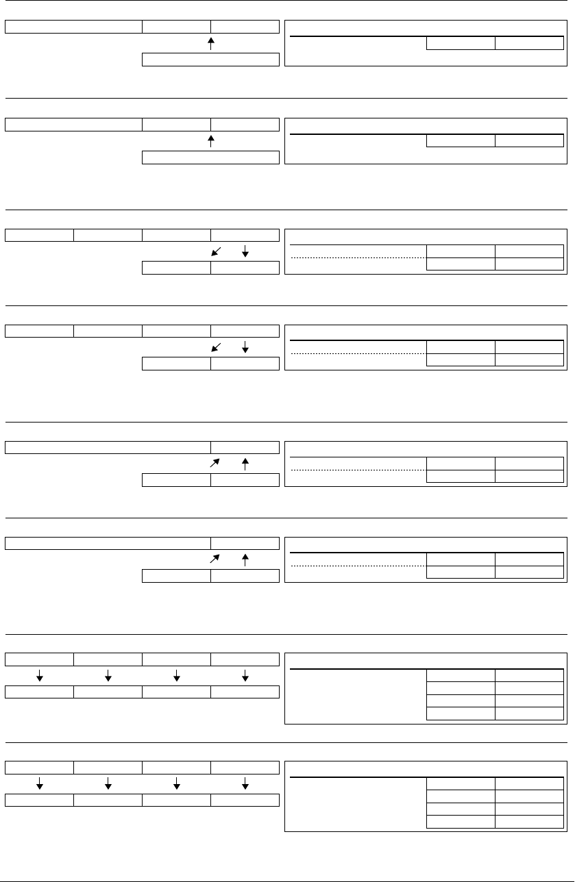
Byte 3
15
Data bus
0#WRL
1
1
1
1
#WRH
0
0
0
0
A0
0
1
0
1
A1
0
0
1
1
No.
1
2
3
4
Data retained
Byte 2 Data retained
Byte 1 Data retained
Byte 0 Data retained
Byte 3 Byte 2 Byte 1 Byte 0
31 0
A[1:0]=01 A[1:0]=11A[1:0]=00 A[1:0]=10
80
41
888000
Source (general-purpose register)
Destination (8-bit device)
2 3
Bus operation
Big-endian
Figure 4.11 Word Data Writing to an 8-bit Device