III PERIPHERAL BLOCK: MONITORED MOBILE ACCESS INTERFACES
S1C33210 FUNCTION PART EPSON B-III-10-7
32 kbps: 20 ms
125 µs 125 µs
0123****45
67****89
Note: *
These bits are "1" for output. Their value does not matter for input.
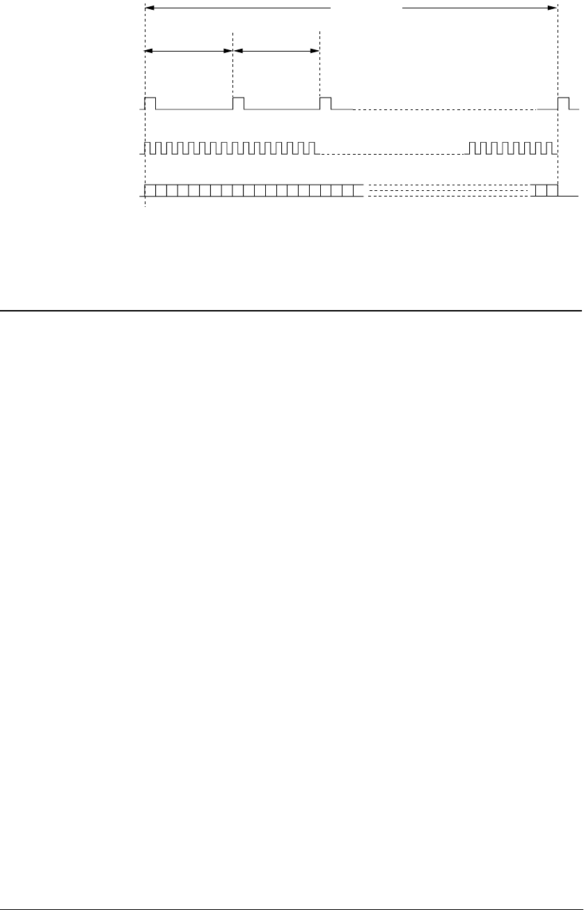
DCD (frame signal)
Frame signal period
PIAFS frame period
CTS (bit clock, 64 kHz)
TXD and RXD (data signals)
(Total 640 bits)
Figure 10.6 PHS Signal Format (5)
UART Communications Mode
Overview
UART communications data transfers use serial IF Ch. 3 asynchronous operation. For further details on using the
serial IF Ch. 3, see Section III-8 "Serial Interfaces."
The communications block modem control register (D[1:0]/0x020002E) controls the DTR and RTS pin output
levels.
Bits in the communications block modem status register (D[11:8]/0x020002A) track the input levels for the DSR,
CTS, DCD, and RI pins as well as transitions for triggering interrupt requests with changes in pin states.
Modem Control Outputs
In UART communications mode, bits in the communications block modem control register
(D[1:0]/0x020002E) control the DTR and RTS pin output levels.
Note that there is no hardware flow control with RTS.
Modem Status Inputs
In UART communications mode, bits in the communications block modem status register
(D[11:8]/0x020002A) track the input levels for the DSR, CTS, DCD, and RI pins using negative logic. Note
that the block does not store these values internally.
Other bits in the same register (D[7:0]/0x020002A) indicate changes in these pin states. A change in the RI
status from "0" to "1," for example, sets the SURI bit (D6/0x020002A) to "1"; one in the reverse direction sets
the SDRI bit (D7/0x020002A) to "1." These bits remain "1" until the software writes "1" to the corresponding
bits. These transitions also trigger modem status change interrupt requests to the CPU if enabled with the
corresponding bits in the communications modem status interrupt enable register (0x02002C).
The above applies to the CTS, DCD, and DSR inputs.
In this mode as in others, setting the GOUTE bit in the communications block input port data register
(D7/0x020000C) to "1" connects the RI input to the GOUT output pin.


