


V DMA BLOCK: HSDMA (High-Speed DMA)
S1C33210 FUNCTION PART EPSON B-V-2-27
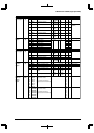
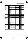
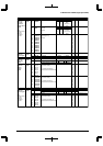
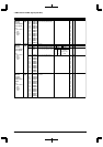
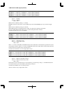
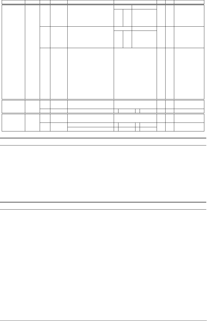
NameAddressRegister name Bit Function Setting Init. R/W Remarks
D3MOD1
D3MOD0
D3IN1
D3IN0
D3ADRH11
D3ADRH10
D3ADRH9
D3ADRH8
D3ADRH7
D3ADRH6
D3ADRH5
D3ADRH4
D3ADRH3
D3ADRH2
D3ADRH1
D3ADRH0
DF
DE
DD
DC
DB
DA
D9
A8
D7
D6
D5
D4
D3
D2
D1
D0
Ch.3 transfer mode
D) Ch.3 destination address
control
S) Invalid
D) Ch.3 destination
address[27:16]
S) Invalid
0
0
0
0
X
X
X
X
X
X
X
X
X
X
X
X
R/W
R/W
R/W
004825A
(HW)
High-speed
DMA Ch.3
high-order
destination
address set-up
register
Note:
D) Dual address
mode
S) Single
address
mode
1
1
0
0
1
0
1
0
D3MOD[1:0] Mode
Invalid
Block
Successive
Single
1
1
0
0
1
0
1
0
D3IN[1:0] Inc/dec
Inc.(no init)
Inc.(init)
Dec.(no init)
Fixed
––
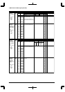
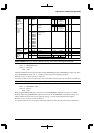
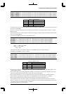
HS3_EN
DF–1
D0
reserved
Ch.3 enable
1 Enable 0 Disable
–
0
–
R/W
Undefined in read.004825C
(HW)
High-speed
DMA Ch.3
enable register
––
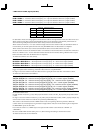
HS3_TF
DF–1
D0
reserved
Ch.3 trigger flag clear (writing)
Ch.3 trigger flag status (reading)
1 Clear 0
No operation
1 Set 0 Cleared
–
0
–
R/W
Undefined in read.004825E
(HW)
High-speed
DMA Ch.3
trigger flag
register
CFK51–CFK50: K5[1:0] pin function selection (D[1:0]) / K5 function select register (0x402C0)
Set the #DMAREQx pin of HSDMA.
Write "1": #DMAREQx input
Write "0": Input port
Read: Valid
CFK50 and CFK51are the function select bits for K50 (#DMAREQ0) and K51 (#DMAREQ1) respectively. When
using the #DMAREQx signal, write "1" to CFK5x to set the K5x port for inputting the signal.
If this bit is set to "0", the pin is set for an input port.
At cold start, CFK5x is set to "0" (input port). At hot start, CFK5x retains the previous status before an initial reset.
CFP16–CFP15: P1[6:5] pin function selection (D[6:5]) / P1 function select register (0x402D4)
Set the #DMAENDx pin of HSDMA.
Write "1": #DMAENDx output
Write "0": I/O port
Read: Valid
When using the #DMAEND0 signal, set the P15 pin for the #DMAEND0 output pin by writing "1" to CFP15.
Similarly, when using the #DMAEND1 signal, set the P16 pin for the #DMAEND1 output pin by writing "1" to
CFP16. Furthermore, direct these pins for output by writing "1" to the corresponding I/O control register.
If CFP1x is set to "0", the pin is set for an I/O port.
At cold start, CFP1x is set to "0" (I/O port). At hot start, CFP1x retains the previous status before an initial reset.