


II CORE BLOCK: BCU (Bus Control Unit)
B-II-4-16 EPSON S1C33210 FUNCTION PART
Ignored
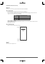
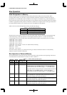
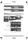
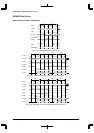
15 Data bus 0#WRL
1
#WRH
X
A0
∗
A1
∗
No.
1
Byte 0
Byte 0
31 0
A[1:0]=∗∗
0
1
8
Bus operation
(X: Not connected/Unused)
Destination (general-purpose register)
Source (8-bit device)
Sign or Zero extension
Little-endian
Byte 0
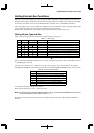
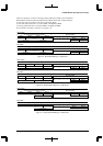
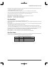
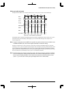
15 Data bus 0#WRL
1
#WRH
1
A0
∗
A1
∗
No.
1 Ignored
Byte 0
31 0
A[1:0]=∗∗
0
1
8
Bus operation
Destination (general-purpose register)
Source (8-bit device)
Sign or Zero extension
Big-endian
Figure 4.16 Byte Data Reading from an 8-bit Device
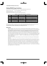
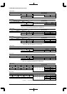
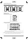
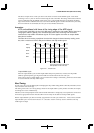
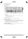
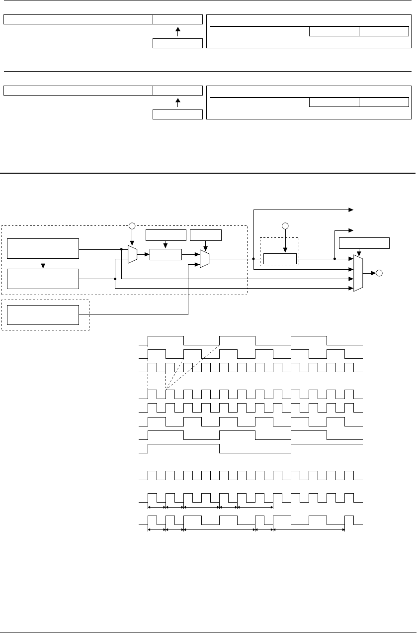
Bus Clock
The bus clock is generated by the BCU using the CPU system clock output from the clock generator.
Figure 4.17 shows the clock system.
High-speed (OSC3)
oscillation circuit
CLKCHGCLKDT[1:0]
BCLKSEL[1:0]
PLLS[1:0] pins
#X2SPD pin
To CPU
OSC3_CLK
OSC3_CLK (PLL: off)
PLL_CLK (PLL: x2 mode)
PLL_CLK (PLL: x4 mode)
A
CPU_CLK (CLKDT = 1/1)
CPU_CLK (CLKDT = 1/2)
CPU_CLK (CLKDT = 1/4)
CPU_CLK (CLKDT = 1/8)
CPU_CLK
BCU_CLK(#X2SPD=H, x1 speed mode)
BCU_CLK(#X2SPD=L, x2 speed mode)
(when the CPU system clock source is OSC3)
∗1
∗1 Access to the internal RAM
∗2 Access to the external memory
∗1
∗1
∗1
∗2 ∗1 ∗2
∗2 ∗1 ∗2
PLL_CLK
A
CPU_CLK
BCU_CLK
Bus clock
PLL
Low-speed (OSC1)
oscillation circuit
CLG
BCU
1/1 or 1/2
1/2-1/8
BCLK pin
Figure 4.17 Clock System