II CORE BLOCK: BCU (Bus Control Unit)
S1C33210 FUNCTION PART EPSON B-II-4-17
Since the bus clock is generated from the CPU system clock (CPU_CLK), the following settings affect the bus clock:
1. Selection of an oscillation circuit (OSC3 or OSC1)
2. PLL configuration (OSC3_CLK ×1, ×2 or ×4)
3. CPU clock division ratio for power saving (1/8, 1/4, 1/2, or 1/1 of OSC3_CLK or PLL_CLK)
Items 2 and 3 apply when the high-speed (OSC3) oscillation circuit is selected as the CPU clock source.
For details about the settings of the system clock, refer to "CLG (Clock Generator)".
Bus clock operation during standby is as follows:
Basic HALT mode:the BCU and bus clock continue operating. DRAM can be refreshed.
HALT2 mode: the BCU and bus clock are stopped.
SLEEP mode: the BCU and bus clock are stopped.
Bus Speed Mode
The CPU - bus clock ratio can be set using the #X2SPD pin as follows:
When #X2SPD = High, ×1 speed mode (CPU - bus clock ratio is 1 : 1) is set. The bus clock and the CPU system clock
will be the same.
When #X2SPD = Low, ×2 speed mode (CPU - bus clock ratio is 2 : 1) is set. In ×2 speed mode, the bus clock will be
dynamically varied according to the memory to be accessed.
• When an external memory area is accessed, the bus clock frequency becomes half of the CPU system clock.
• When the internal RAM/ROM area is accessed, the bus clock frequency becomes equal to the CPU system clock.
In ×1 speed mode, area 1 (internal I/O area) is accessed in 4 cycles of the CPU system clock, while in ×2 speed mode,
the number of access cycles can be selected using A1X1MD (D3) / BCLK select register (0x4813A).
When A1X1MD = "1", area 1 is accessed in 2 cycles of the CPU system clock.
When A1X1MD = "0", area 1 is accessed in 4 cycles of the CPU system clock. (default)
Bus Clock Output
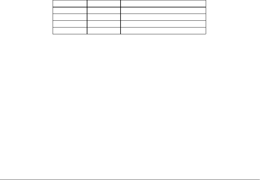
The bus clock is also output from the BCLK pin to an external device. The BCLK output clock can be selected from
among four types using BCLKSEL[1:0] (D[1:0]) / BCLK select register (0x4813A).
Table 4.12 Selection of BCLK Output Clock
BCLKSEL1 BCLKSEL0 Output clock
1 1 PLL_CLK (PLL output clock)
1 0 OSC3_CLK (OSC3 oscillation clock)
0 1 BCU_CLK (BCU operating clock)
0 0 CPU_CLK (CPU operating clock)


