


II CORE BLOCK: DBG (Debug Unit)
S1C33210 FUNCTION PART EPSON B-II-7-1
II-7 DBG (Debug Unit)
Debug Circuit
The C33 Core Block has a built-in debug circuit.
This functional block is provided to simply realize an advanced software development environment.
Note: The debug circuit does not work during normal operation. To construct a software development
environment using the debug circuit, the S5U1C33000H (In-Circuit Debugger for S1C33 Family) is
separately required.
I/O Pins of Debug Circuit
Six pins used to exclusively connect the S5U1C33000H (In-Circuit Debugger for S1C33 Family) are reserved for the
debug circuit. The I/O voltage level of these pins is 3.3 V.
Table 7.1 lists the I/O pins of the debug circuit.
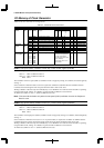
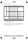
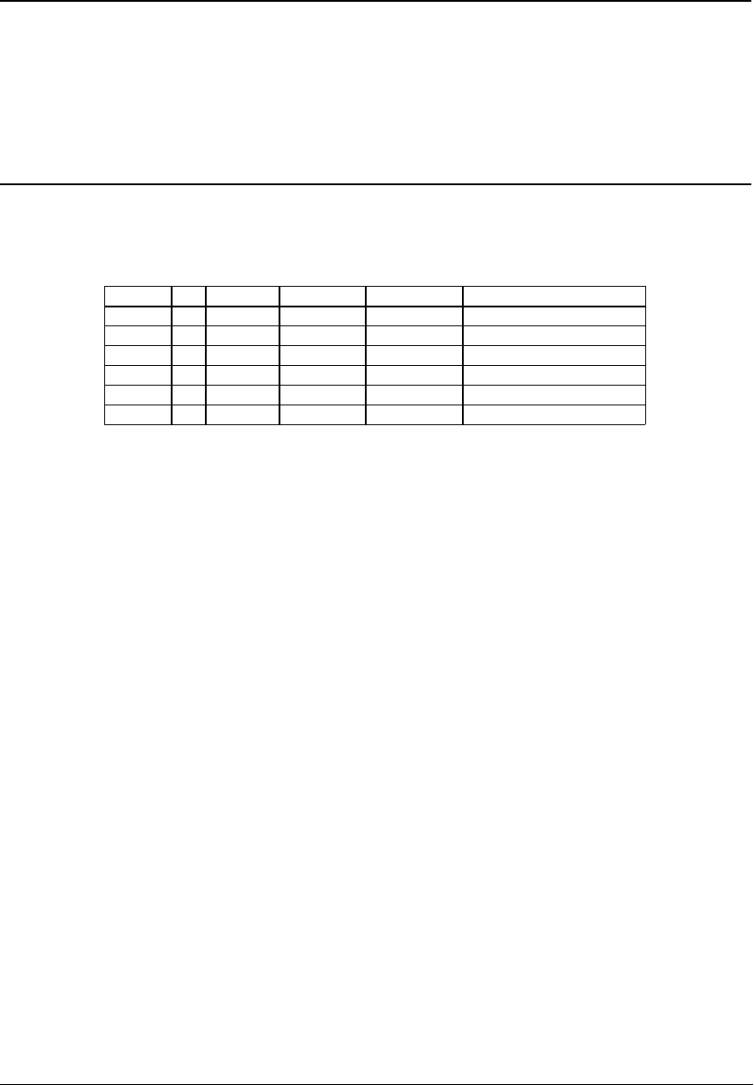
Table 7.1 I/O Pins of Debug Circuit
Pin name I/O Pull-up Initial status Voltage level Function
DCLK O – 1 3.3 V Clock output for debugging
DST2 O – 0 3.3 V Status output 2 for debugging
DST1 O – 1 3.3 V Status output 1 for debugging
DST0 O – 1 3.3 V Status output 0 for debugging
DPCO O – 1 3.3 V PC output for debugging
DSIO I/O With pull-up 1 (Input) 3.3 V Serial I/O for debugging
The DCLK, DST[2:0] and DPCO outputs are extended functions of the I/O port pins P14, P1[2:0] and P13,
respectively. At initial reset, these pins are set as debug signal outputs.
If the debug circuit is not used, these pins can be used for I/O ports or the redefined peripheral circuits by writing "0"
to CFEX[1:0] (D[1:0]) / Port function extension register (0x402DF). Refer to "I/O Ports (P Ports)" for the pin
functions.
Note: When these pins are set as debug signal outputs, only the S5U1C33000H (In-Circuit Debugger for
S1C33 Family) can be connected to these pins. Leave these pins open if the S5U1C33000H is not
connected. For connecting the S5U1C33000H, refer to the "S1C33 Family In-Circuit Debugger
Manual".
Furthermore, the pin status is fixed as shown in the above table after a user reset.