


III PERIPHERAL BLOCK: INPUT/OUTPUT PORTS
B-III-9-16 EPSON S1C33210 FUNCTION PART
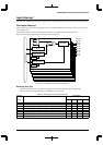
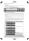
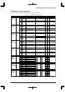
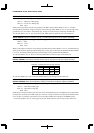
Table 9.9 Control Bits for IDMA Transfer
System IDMA request bit IDMA enable bit
FPT7 RP7(D7/0x40293) DEP7(D7/0x40297)
FPT6 RP6(D6/0x40293) DEP6(D6/0x40297)
FPT5 RP5(D5/0x40293) DEP5(D5/0x40297)
FPT4 RP4(D4/0x40293) DEP4(D4/0x40297)
FPT3 RP3(D3/0x40290) DEP3(D3/0x40294)
FPT2 RP2(D2/0x40290) DEP2(D2/0x40294)
FPT1 RP1(D1/0x40290) DEP1(D1/0x40294)
FPT0 RP0(D0/0x40290) DEP0(D0/0x40294)
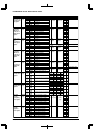
If the IDMA request and enable bits are set to "1", IDMA is invoked through generation of an interrupt factor.
No interrupt request is generated at that point. An interrupt request is generated after the DMA transfer is
completed. The registers can also be set so as not to generate an interrupt, with only DMA transfers performed.
For details on IDMA transfers and interrupt control upon completion of IDMA transfer, refer to "IDMA
(Intelligent DMA)".
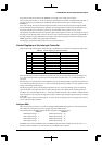
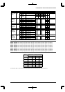
Trap vectors
The trap-vector address of each input default interrupt factor is set as follows:
FPT0 input interrupt: 0x0C00040
FPT1 input interrupt: 0x0C00044
FPT2 input interrupt: 0x0C00048
FPT3 input interrupt: 0x0C0004C
FPK0 input interrupt: 0x0C00050
FPK1 input interrupt: 0x0C00054
FPT4 input interrupt: 0x0C00110
FPT5 input interrupt: 0x0C00114
FPT6 input interrupt: 0x0C00118
FPT7 input interrupt: 0x0C0011C
The base address of the trap table can be changed using the TTBR register (0x48134 to 0x48137).