


III PERIPHERAL BLOCK: SERIAL INTERFACE
B-III-8-10 EPSON S1C33210 FUNCTION PART
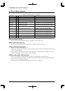
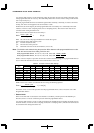
Ch.0 receive data buffer full: RDBF0 (D0) / Serial I/F Ch.0 status register (0x401E2)
Ch.1 receive data buffer full: RDBF1 (D0) / Serial I/F Ch.1 status register (0x401E7)
Ch.2 receive data buffer full: RDBF2 (D0) / Serial I/F Ch.2 status register (0x401F2)
Ch.3 receive data buffer full: RDBF3 (D0) / Serial I/F Ch.3 status register (0x401F7)
This bit is set to "1" (buffer full) when the MSB of serial data is received and the data in the shift register is
transferred to the receive data register, indicating that the received data can be read out. When the data is read
out, the bit is reset to "0".
The following describes a receive operation in the master and slave modes.
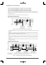
• Clock-synchronized master mode
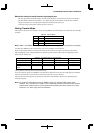
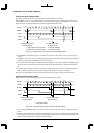
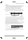
Figure 8.6 shows a receive timing chart in the clock-synchronized master mode.
#SCLKx
SINx
RXDx
RDBFx
#SRDYx
Receive-buffer full
interrupt request
Receive-buffer full
interrupt request
A First data is read.
D0 D1 D6 D7 D0 D1 D6 D7 D0 D1
A
1st data 2nd data
Figure 8.6 Receive Timing Chart in Clock-Synchronized Master Mode
1. If the #SRDYx signal from the slave is on a high level, the master waits until it turns to a low level (ready to
receive).
2. If #SRDYx is on a low level, synchronizing clock input to the serial interface begins. The synchronizing
clock is also output from the #SCLKx pin to the slave device.
3. The slave device outputs each bit of data synchronously with the falling edges of the clock. The LSB is output
first.
4. This serial interface takes the SIN input into the shift register at the rising edges of the clock. The data in the
shift register is sequentially shifted as bits are taken in. This operation is repeated until the MSB of data is
received.
5. When the MSB is taken in, the data in the shift register is transferred to the receive data register, enabling
the data to be read out.
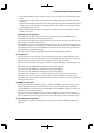
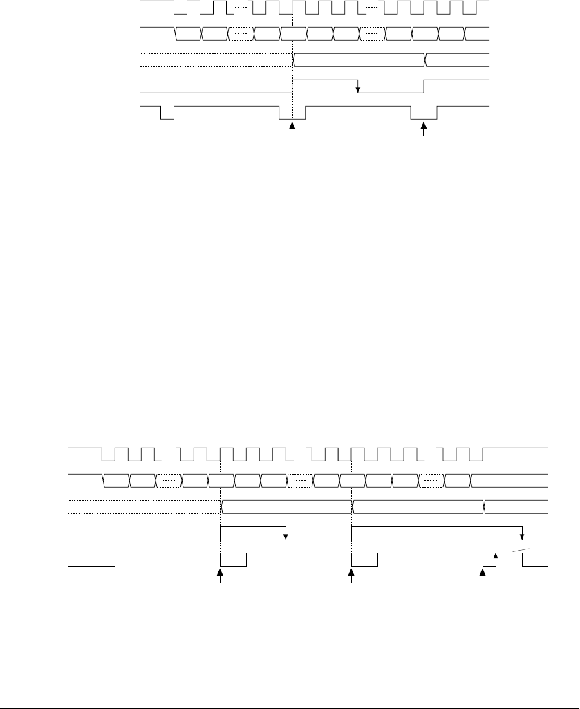
• Clock-synchronized slave mode
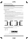
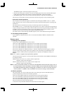
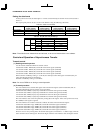
Figure 8.7 shows a receive timing chart in the clock-synchronized slave mode.
#SCLKx
SINx
RXDx
RDBFx
#SRDYx
Receive-buffer full
interrupt request
Receive-buffer full
interrupt request
A
B
First data is read.
3rd data is read.
C
D
An overrun error occurs because the receive operation has completed when RDBFx = "1".
Send the busy signal to the master device to stop the clock.
D0 D1 D6 D7 D0 D1 D6 D7 D0
Receive-buffer full
interrupt request
A
D1 D6 D7
1st data 2nd data 3rd data
C
D
B
Figure 8.7 Receive Timing Chart in Clock-Synchronized Slave Mode