


II CORE BLOCK: BCU (Bus Control Unit)
S1C33210 FUNCTION PART EPSON B-II-4-19
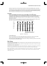
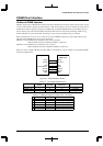
The above example shows a read cycle when a wait mode is inserted via the #WAIT signal. A wait mode
consisting of 0 to 7 cycles can also be inserted using the wait control bits. The settings of these bits can also be
used in combination with the #WAIT signal. In this case as well, the #WAIT signal is sampled at the falling
edge of the transition of BCLK. However, even when the #WAIT signal is inactive before the wait cycles set by
the wait control bits are terminated, the read cycle is not terminated at that time.
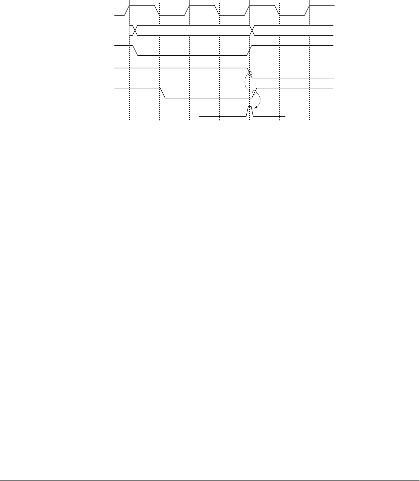
Precaution
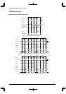
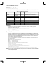
#CE and address hold times at the rising edge of the #RD signal
In read cycles of this BCU, the rise of the #RD signal, negating the chip enable (#CExx) signal and
changing the address (A[23:0]) occur simultaneously at the same clock edge. No hold time is
inserted to the chip enable and address signals. The same applies even when an output disable
delay time is inserted.
Therefore when connecting a peripheral circuit, which changes its internal state by reading, to the
bus, take a measure to insert a delay to the address and chip enable signals.
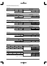
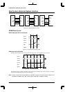
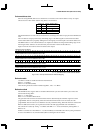
BCLK
A[23:0]
#CE4
#CE7
#RD
addr
Hazard occurrence.
This hazard causes an erroneous
RD operation on the next area.
Figure 4.21 Trouble Case
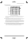
Output disable cycle
When an output disable cycle (set with output disable delay time parameter) is inserted, the chip enable
(#CExx) signal temporarily goes high. This makes an interval between the next read cycle.
Note, however, that no output disable cycle is inserted when reading is continuously performed to the area that
is accessed with the same chip enable signal.
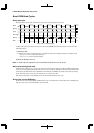
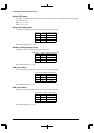
Bus Timing
In read cycles, the rise of the #RD signal and changing the chip enable setting (#CE4 to #CE10) and address (A23 to
A0) occur at the same clock edge.
This timing is the same even if a long setting is made for the output disable cycle by the bus controller, for example,
and changeover occurs simultaneously.
Therefore, when an I/O peripheral circuit whose internal information is changed by a read operation is connected to
the C33 bus, appropriate measures must be taken to insert a delay for the address and chip enable signals.
With an output disable cycle, there is normally a gap between one read cycle and the next. Note, however, that this
output disable cycle is not inserted in the case of consecutive reads in a memory area for which the same chip
enable signal is output.