III PERIPHERAL BLOCK: SERIAL INTERFACE
B-III-8-18 EPSON S1C33210 FUNCTION PART
Receive control
(1) Enabling receive operations
Use the receive-enable bit RXENx for receive control.
Ch.0 receive-enable: RXEN0 (D6) / Serial I/F Ch.0 control register (0x401E3)
Ch.1 receive-enable: RXEN1 (D6) / Serial I/F Ch.1 control register (0x401E8)
Ch.2 receive-enable: RXEN2 (D6) / Serial I/F Ch.2 control register (0x401F3)
Ch.3 receive-enable: RXEN3 (D6) / Serial I/F Ch.3 control register (0x401F8)
When receiving enabled by writing "1" to this bit, clock input to the shift register is enabled (ready for input),
meaning that it is ready to receive data.
Receive operations are disabled by writing "0" to RXENx.
Note: Do not set RXENx to "0" during a receive operation.
(2) Receive procedure
This serial interface has a receive shift register and a receive data register (receive data buffer) that are
provided independently of those used for transmit operations.
Ch.0 receive data: RXD0[7:0] (D[7:0]) / Serial I/F Ch.0 receive data register (0x401E1)
Ch.1 receive data: RXD1[7:0] (D[7:0]) / Serial I/F Ch.1 receive data register (0x401E6)
Ch.2 receive data: RXD2[7:0] (D[7:0]) / Serial I/F Ch.2 receive data register (0x401F1)
Ch.3 receive data: RXD3[7:0] (D[7:0]) / Serial I/F Ch.3 receive data register (0x401F6)
Receive data can be read out from this register.
A status bit is also provided to indicate the status of the receive data register.
Ch.0 receive data buffer full: RDBF0 (D0) / Serial I/F Ch.0 status register (0x401E2)
Ch.1 receive data buffer full: RDBF1 (D0) / Serial I/F Ch.1 status register (0x401E7)
Ch.2 receive data buffer full: RDBF2 (D0) / Serial I/F Ch.2 status register (0x401F2)
Ch.3 receive data buffer full: RDBF3 (D0) / Serial I/F Ch.3 status register (0x401F7)
This bit is set to "1" (buffer full) when data is transferred from the shift register to the receive data register
after the stop bit is sampled (the second bit if two stop bits are used), indicating that the received data can be
read out. When the data is read out, the bit is reset to "0".
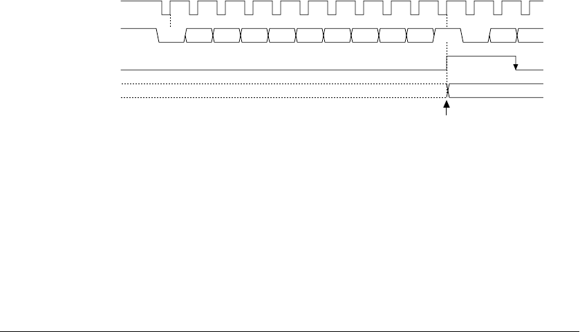
Figure 8.13 shows a receive timing chart in the asynchronous mode.
Example: Data length 8 bits
Stop bit 1 bit
Parity bit Included
Sampling clock
SOUTx
RDBFx
RXDx
Receive-buffer full
interrupt request
S1
S2
Start bit
Stop bit
P
A
Parity bit
First data is read.
S1 D0 D1 S1 D0 D1D2 D3 D4 D5 D6 D7 P S2
A
1st data
Figure 8.13 Receive Timing Chart in Asynchronous Mode
1. The serial interface starts sampling when the start bit is input (SINx = low).
2. When the start bit is sampled at the first rising edge of the sampling clock, each bit of receive data is taken
into the shift register, beginning with the LSB at each rising edge of the subsequent clock. This operation is
repeated until the MSB of data is received.
3. When the MSB is taken in, the parity bit that follows is also taken in (if EPRx = "1").
4. When the stop bit is sampled, the data in the shift register is transferred to the receive data register,
enabling the data to be read out.
The parity is checked when data is transferred to the receive data register (if EPRx = "1").


