


1 OUTLINE
S1C33210 PRODUCT PART EPSON A-5
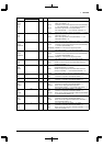
1.3.2 Pin Functions
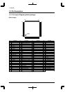
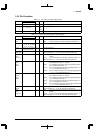
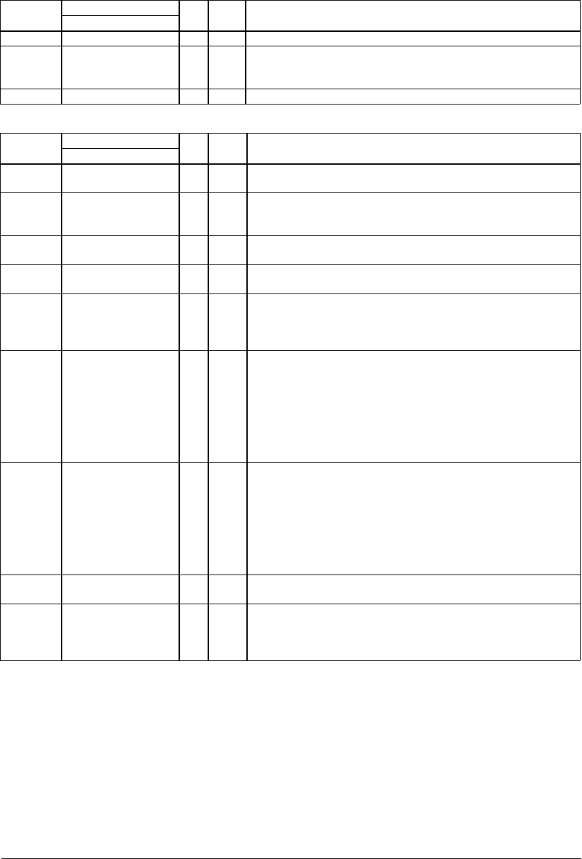
Table 1.3.1 List of Pins for Power Supply System
Pin name Pin No. I/O Pull-up Function
QFP15-128
VDD 8, 27, 47, 74, 93, 111 ––Power supply (+)
VSS 3, 22, 39, 54, 67, 90,
102, 104
– (104
Pull-
down)
Power supply (-); GND
AVDD 30 ––Analog system power supply (+); AVDD = VDD
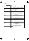
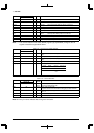
Table 1.3.2 List of Pins for External Bus Interface Signals
Pin name Pin No. I/O Pull-up Function
QFP15-128
A0
#BSL
55 O – A0: Address bus (A0) when SBUSST(D3/0x4812E) = "0" (default)
#BSL: Bus strobe (low byte) signal when SBUSST(D3/0x4812E) = "1"
A[23:1] 56-58, 63-66, 69, 70, 72,
75, 78, 81, 84, 85, 87-89,
91, 73, 76, 79, 82
O – Address bus (A1 to A23)
D[15:0] 7, 10, 12, 14, 16, 18, 25, 26,
36-38, 40-42, 45, 46
I/O – Data bus (D0 to D15)
#CE10EX
#CE9&10EX
34 O – Area 10 chip enable for external memory
* When CEFUNC[1:0] = "1x", this pin outputs #CE9+#CE10EX signal.
#CE9
#CE17
#CE17&18
48 O – #CE9: Area 9 chip enable when CEFUNC[1:0](D[A:9])/0x48130) = "00"
(default)
#CE17: Area 17 chip enable when CEFUNC[1:0](D[A:9])/0x48130) = "01"
* When CEFUNC[1:0] = "1x", this pin outputs #CE17+#CE18 signal.
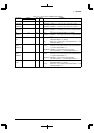
#CE8
#RAS1
#CE14
#RAS3
53 O – #CE8: Area 8 chip enable when CEFUNC[1:0](D[A:9])/0x48130) = "00"
and A8DRA(D8/0x48128) = "0" (default)
#RAS1: Area 8 DRAM row strobe when CEFUNC[1:0](D[A:9])/0x48130) =
"00" and A8DRA(D8/0x48128) = "1"
#CE14: Area 14 chip enable when CEFUNC[1:0](D[A:9])/0x48130) = "01"
or "1x" and A14DRA(D8/0x48122) = "0"
#RAS3: Area 14 DRAM row strobe when CEFUNC[1:0](D[A:9])/0x48130)
= "01"or "1x" and A14DRA(D8/0x48122) = "1"
#CE7
#RAS0
#CE13
#RAS2
49 O – #CE7: Area 7 chip enable when CEFUNC[1:0](D[A:9])/0x48130) = "00"
and A7DRA(D7/0x48128) = "0" (default)
#RAS0: Area 7 DRAM row strobe when CEFUNC[1:0](D[A:9])/0x48130) =
"00" and A7DRA(D7/0x48128) = "1"
#CE13: Area 13 chip enable when CEFUNC[1:0](D[A:9])/0x48130) = "01"
or "1x" and A13DRA(D7/0x48122) = "0"
#RAS2: Area 13 DRAM row strobe when CEFUNC[1:0](D[A:9])/0x48130)
= "01" or "1x" and A13DRA(D7/0x48122) = "1"
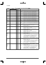
#CE6
#CE7&8
52 O – Area 6 chip enable
* When CEFUNC[1:0] = "1x", this pin outputs #CE7+#CE8 signal.
#CE5
#CE15
#CE15&16
71 O – #CE5: Area 5 chip enable when CEFUNC[1:0](D[A:9])/0x48130) = "00"
(default)
#CE15: Area 15 chip enable when CEFUNC[1:0](D[A:9])/0x48130) = "01"
* When CEFUNC[1:0] = "1x", this pin outputs #CE15+#CE16 signal.