


III PERIPHERAL BLOCK: MONITORED MOBILE ACCESS INTERFACES
B-III-10-26 EPSON S1C33210 FUNCTION PART
BMODE, BHALF, FMODE: PHS signal format (D[2:0]) / Communications block PHS mode settings
register (0x0200010)
These bits specify the interface signal format for PHS communications. They are ignored for other communications
modes.
Use only the combinations given.
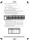
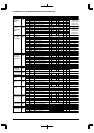
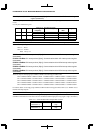
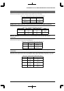
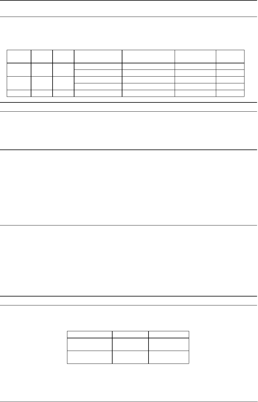
Table 10.14 PHS Signal Formats
BMODE BHALF FMODE Frame Signal
Frequency
Bit Clock Frequency Data Transfer
Rate
Figure
0 0 0 200 Hz (5 ms) 32 kHz 32 kbps Figure 10.2
200 Hz (5 ms) 64 kHz 64 kbps Figure 10.3
1 0 1 8 kHz 32 kHz 32 kbps Figure 10.4
8 kHz 64 kHz 64 kbps Figure 10.5
1 1 1 8 kHz 64 kHz 32 kbps Figure 10.6
PHSRST, PDCRST, HDLRST: PHS/PDC/HDLC block reset (D[2:0]) / Software reset register (0x0200002)
Resets the corresponding block.
Write "1": Reset
Write "0": Invalid
Read: Always "0"
CP0EN4–CP0EN0: CP0 interrupt select (D[4:0]) / Communications block CP0 interrupt select register
(0x0200020)
CP1EN4–CP1EN0: CP1 interrupt select (D[4:0]) / Communications block CP1 interrupt select register
(0x0200022)
CP2EN4–CP2EN0: CP2 interrupt select (D[4:0]) / Communications block CP2 interrupt select register
(0x0200024)
CP3EN4–CP3EN0: CP3 interrupt select (D[4:0]) / Communications block CP3 interrupt select register
(0x0200026)
CP4EN4–CP4EN0: CP4 interrupt select (D[4:0]) / Communications block CP4 interrupt select register
(0x0200028)
These bits map the interrupt groups UNIT0 to UINT4 to the interrupt pins CP0 to CP4.
CP0 = CP0EN0*UINT0 + CP0EN1*UINT1 + CP0EN2*UINT2 + CP0EN3*UINT3 + CP0EN4*UINT4
CP1 = CP1EN0*UINT0 + CP1EN1*UINT1 + CP1EN2*UINT2 + CP1EN3*UINT3 + CP1EN4*UINT4
CP2 = CP2EN0*UINT0 + CP2EN1*UINT1 + CP2EN2*UINT2 + CP2EN3*UINT3 + CP2EN4*UINT4
CP3 = CP3EN0*UINT0 + CP3EN1*UINT1 + CP3EN2*UINT2 + CP3EN3*UINT3 + CP3EN4*UINT4
CP4 = CP4EN0*UINT0 + CP4EN1*UINT1 + CP4EN2*UINT2 + CP4EN3*UINT3 + CP4EN4*UINT4
For further details on interrupt groups UNIT0 to UINT4 and the interrupt pins CP0 to CP4 X, see "Mobile Access
Interface Interrupt Outputs."
MOPORT3, MOPORT2:
Output port data (D[3:2]) / Communications block output port data register (0x020000A)
For communications macro select (MCRS) register (D[1:0]/0x200000) settings other than 00–that is, HDLC, PDC,
and PHS communications modes–these bits drive the RTS and DTR output pins using negative logic. (See Table.)
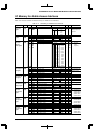
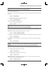
Table 10.15 Communications Block Outputs RTS and DTR
Output port data Output pins Output level
MOPORT3 = 1
MOPORT3 = 0
RTS Low
High
MOPORT2 = 1
MOPORT2 = 0
DTR Low
High