


III PERIPHERAL BLOCK: SERIAL INTERFACE
S1C33210 FUNCTION PART EPSON B-III-8-3
Method for setting the serial-interface input/output pins
All of the pins used in the serial interface are shared with I/O ports. At cold start, they are all set for I/O port
pins P0x (function select bit Pxx, CFPxx = "0"). When using the serial interface, make function select bit
settings for the pins used, according to the channel and transfer mode to be used.
At hot start, the pins retain their status from prior to the reset.
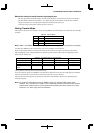
Setting Transfer Mode
The transfer mode of the serial interface can be set using SMDx[1:0] individually for each channel as shown in Table
8.2 below.
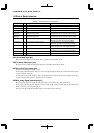
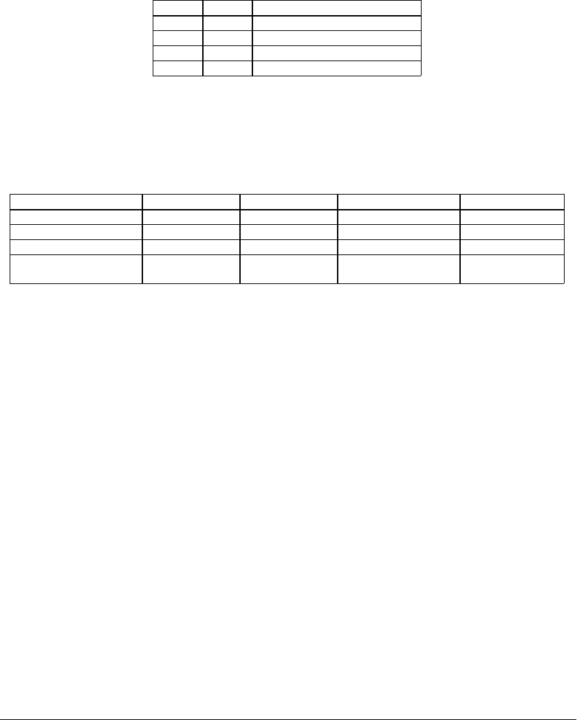
Table 8.2 Transfer Mode
SMDx1 SMDx0 Transfer mode
1 1 8-bit asynchronous mode
1 0 7-bit asynchronous mode
0 1 Clock-synchronized slave mode
0 0 Clock-synchronized master mode
Note: SMD11 and SMD31 must be "1" because Ch. 1 and Ch. 3 support only asynchronous operation.
At initial reset, SMDx becomes indeterminate, so be sure to initialize it in the software.
When using the IrDA interface, set the transfer mode for the asynchronous 7-bit or asynchronous 8-bit mode.
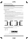
The input/output pins are configured differently, depending on the transfer mode. The pin configuration in each
mode is shown in Table 8.3.
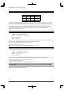
Table 8.3 Pin Configuration by Transfer Mode
Transfer mode SINx SOUTx #SCLKx #SRDYx
8-bit asynchronous Data input Data output Clock input/P port P port
7-bit asynchronous Data input Data output Clock input/P port P port
Clock-synchronized slave Data input Data output Clock input Ready output
Clock-synchronized
master
Data input Data output Clock output Ready input
All four pins are used in the clock-synchronized mode.
In the asynchronous mode, since #SRDYx is unused, P03 (or P23, P24) can be used as an I/O (P) port. In addition,
when an external clock is not used, P02 (or P15, P25) can also be used as an I/O port.
The I/O control and data registers for the I/O ports used in the serial interface can be used as general-purpose
read/write registers.
Note: To enable the IrDA interface to be set, IRMDx[1:0] (D[1:0]) / Serial I/F IrDA register (Ch.0:
0x401E4, Ch.1: 0x401E9, Ch.2: 0x401F4, Ch.3: 0x401F9) is provided. Since these bits become
indeterminate at initial reset, be sure to initialize them by writing "00" when using as the normal
interface or "10" when using as the IrDA interface.