II CORE BLOCK: BCU (Bus Control Unit)
S1C33210 FUNCTION PART EPSON B-II-4-31
Normally, DRAM specifications require that the contents of all row addresses be refreshed within a certain time
before and after a self-refresh. To meet this requirement, make sure a CAS-before-RAS refresh is executed by
a program. In this case, set the 8-bit programmable timer 0 so that the contents of all row addresses are
refreshed within a predetermined time.
Note: If read from or write to the DRAM under a self-refresh is attempted, the BCU keeps #RAS and
#HCAS/#LCAS low as it executes a read/write cycle. Other bus signals than #RAS and
#HCAS/#LCAS (e.g., address, data, and control signals) change their state according to the
specified conditions. Since said attempt initiates an invalid access to the DRAM, do not read from
or write to the DRAM during a self-refresh.
Releasing External Bus
The external bus is normally controlled by the CPU, but the BCU is designed to release control of the bus ownership
to an external device. This function is enabled by writing "1" to SEMAS (D2) / Bus control register (0x4812E)
(disabled by default). The #BUSREQ (P34) and #BUSACK (P35) pins are used for control of the bus ownership.
To direct the P34 and P35 pins for input/output of the #BUSREQ and #BUSACK signals, write "1" to CFP34 (D4)
and CFP35 (D5) / P3 function select register (0x402DC [Byte]).
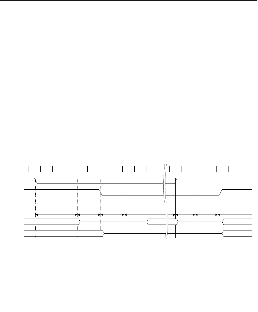
Sequence in which control of the bus is released
This sequence is described below.
1. The external bus master device requesting control of the bus ownership lowers the #BUSREQ pin.
2. The CPU keeps monitoring the status of the #BUSREQ pin, so that when this pin is lower, the CPU
terminates the bus cycle being executed and places the signals listed below in high-impedance state one
cycle later:
A[23:0], D[15:0], #RD, #WRL, #WRH, #HCAS, #LCAS, #CExx
Then the CPU lowers the #BUSACK pin to inform the external device that control of the bus ownership has
been released.
3. One cycle later, the external bus starts its own bus cycle. The external bus master must hold the #BUSREQ
pin low until the bus cycle is completed.
4. After completing the necessary bus cycles, the external bus master places the bus in high-impedance state
and releases the #BUSREQ pin back high.
5. After confirming that the #BUSREQ pin is raised again, the CPU raises the #BUSACK pin one cycle later
and resumes the processing that has been suspended.
BCLK
#BUSREQ
#BUSACK
D[15:0]
A[23:0]
#RD, #WR
Synchronization
Synchronization
The S1C33
terminates the bus
cycle being executed.
The S1C33
controls bus cycles.1 cycle 1 cycle
Hi-Z
1 cycle
The external bus master
controls bus cycles.
Figure 4.38 External Bus Release Timing
If control of the bus ownership is requested during a DMA transfer by the internal DMA controller, the DMA
transfer under way is suspended at a break in data to accept the request for bus ownership control. The DMA
transfer that has been kept pending is restarted when the CPU gains control of the bus ownership.


