


Architecture
7
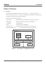
Chapter 2 Architecture
2.1 Overview
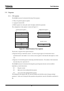
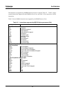
A block diagram of the R3900 Processor Core is shown in Figure 2-1. It includes the CPU core, an
instruction cache and a data cache. You can select an optimum data and instruction cache configuration for
your system from among a variety of possible configurations.
The CPU Core comprises the following blocks:
• CPU registers : General-purpose register, HI/LO register and program counter (PC).
• CP0 registers : Registers for system control coprocessor (CP0) functions.
• ALU/Shifter : Computational unit.
• MAC : Computational unit for multiply/add.
• Bus interface unit : Control bus interface between CPU core and external circuit.
• Memory management unit : Direct segment mapping memory management unit.
Figure 2-1. Block Diagram of the R3900 Processor Core
CPU core
R3900 Processor Core
Memory
Management Unit
MAC
ALU/Shifter
CP0 Register
CPU Register
Bus Interface Unit
Data CacheInstruction Cache