


Architecture
63
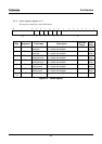
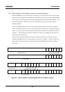
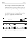
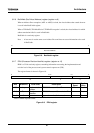
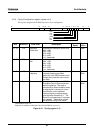
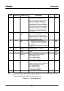
Bits Mnemonic Field name Description
Value on
Reset
Read/
Write
8 Halt
††
Halt Setting this bit to 1 puts the R3900
Processor Core in Halt mode. This
state is canceled by a Reset exception
when a reset signal is received, or
when cancelled by a non-maskable
interrupt signal or interrupt signal that
clears the Halt bit to 0. The Halt bit is
cleared even if interrupts are masked.
Data cache snoops are not possible in
Halt mode. Halt mode reduces power
consumption to a greater extent than
Doze mode.
0 Read/
Write
7 Lock Lock Config
register
Setting this bit to 1 prevents further
writes to the Config register. This bit
is cleared to 0 by a Reset exception.
If a store instruction is used to set other
bits at the same time as the Lock bit,
the other settings are valid.
0 Reset
6 DCBR Data Cache Burst
Refill
1:Indicates that the value in the
DRSize field of the Config register
should be used as the data cache
refill size.
0:The data cache refill size is 1 word (4
bytes).
0 Read/
Write
5 ICE Instruction Cache
Enable
Setting this bit to 1 enables the
instruction cache.
1 Read/
Write
4 DCE Data Cache
Enable
Setting this bit to 1 enables the data
cache.
1 Read/
Write
3-2 IRSize Instruction Burst
Refill Size
These bits designate the instruction
cache burst refill size as follows.
00: 4 words (16 bytes)
01: 8 words (32 bytes)
10: 16 words (64 bytes)
11: 32 words (128 bytes)
00 Read/
Write
1-0 DRSize Data Burst Refill
Size
These bits indicate the data cache
burst refill size as follows. (This
setting is valid only when the DCBR bit
in the Config register is set to 1.)
00: 4 words (16 bytes)
01: 8 words (32 bytes)
10: 16 words (64 bytes)
11: 32 words (128 bytes)
00 Read/
Write
31-22,
15-12
0 Ignored on write; 0 when read 0 Read
Note :
†
After modifications to DCBR, ICE, DCE, IRSize or DRSize, the new cache configuration takes effect after
completion of the currently executing bus operation (cache refill).
†† Operation is undefined when both Doze bit and Halt bit are set to 1.
Figure 6-10. Config register(2/2)