


SECTION 2
DETAILED APPLICATION EXAMPLES
Memory Addressing
One of
the
necessary functions of the microprocessor bus is
to interface with the memory where the program is stored.
ROM
and EPROM memories are typically used
to
store pro-
grams while static
and
dynamic
RAMS
are
generally used for
data memory. The
following discussions cover the interfacing
to be
used
for these types of memory.
ROM
- EPROM ADDRESSING
Later in
this
Appendix a section is devoted
to
an
ap-
proach for developing a chart showing memory device
compatibility for the 8085A. However, there is one area not
included that will be discussed here, that
is,
unbuffered inter-
facing to standard
ROM
or EPROM memories.
To
use
an
unbuffered interface to
ROM
or EPROM
it
is necessary to
understand a particular characteristic of the 8085A.
The
8085A
has
a period of time,
T4
through T6 of the op code
fetch cycle and certain instructions, where addresses
A8
through
A15
are
undefined.
Be
careful about this. Not having
addresses stable
and
using
an
address. select method that
would randomly turn
on
memory devices will cause bus
contention and reliability problems in the unbuffered system.
In
the memory compatibility section of this Application Note,
a minimum (unbuffered
MCS-85 family and medium system
(at least one
level
of buffering) configurations
are
considered.
These configurations do not
have
bus
contention problems.
In
the minimum system only MCS-85 components will
be
discussed where addresses
are
latched
on
the falling edge of
ALE,
thus ignoring any extraneous address transitions. The
medium system
is
assumed to
have
data buffers that are
enabled
only at the proper time, thus again preventing any
bus contention problems. What about the user who wants to
use
standard
ROM
or
EPROM
without buffering?
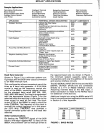
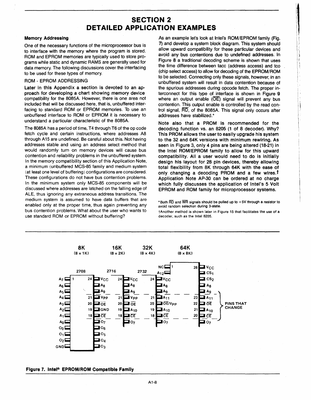
8K
(8
x
1K)
16K
(8 x
2K)
32K
(8
x
4K)
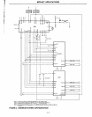
2708
2716
2732
Vee
vee
AS
AS
Ag
Ag_
-
Vpp
Vpp
OE
DE
GND
A10
CE
CE
07
07
06
05
04
03
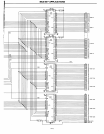
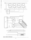
Figure
7.
Intel\!) EPROM/ROM Compatible Family
A1·8
As
an
example let's look at Intel's ROM/EPROM family
(Fig.
7)
and develop a system block diagram. This system should
allow
upward compatibility for these particular devices and
avoid any bus contentions due to undefined addresses.
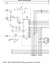
In
Figure 8 a traditional decoding scheme is shown that uses
the time difference between tacc (address access)
and
tco
(chip
select access) to allow for decoding of the EPROM/ROM
to be selected. Connecting only these signals, however, in
an
unbuffered system will result
in
data contention because of
the spurious addresses during opcode fetch. The proper
in-
terconnect for this type of interface is shown
in
Figure 9
where
an
output enable (OE)
Signal
will prevent any bus
contention. This output enable is controlled by the read
con-
trol signal,
RD,
of the 8085A. This signal only occurs after
addresses have stabilized.*
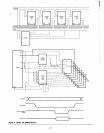
Note also
that
a PROM is recommended
for
the
decoding
function
vs. an 8205
(1
of
8 decoder). Why?
This
PROM
allows
the user
to
easily upgrade
his
system
to
the
32 and 64K versions
with
minimum
rewiring. As
seen
in
Figure
3,
only 4 pins are being altered
(18-21)
in
the
Intel ROM/EPROM
family
to
a.llow for
this
upward
compatibility;
All a user would need
to
do
is
initially
design
his
layout
for
28 pin devices, thereby allowing
total
flexibility
from 8K through 64K
with
the
ease
of
only
changing a decoding PROM
and·
a few wires. t
Application Note Ap·30 can be ordered at no charge
which
fully
discusses
the
application
of
Intel's
5
Volt
EPROM and
ROM
family
for
microprocessor
systems.
• Both
AD
and
WR
signals should be pulled up to + 5V through a resistor to
avoid random
selection during 3·state.
tAnother
method is shown later in Figure 15 that facilitates the use
of
a
decoder, such
as
the Intel
S205.
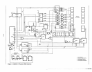
NC
AS
Ag
A11
OElVpp
A10
CE
07
64K
(8 x
8K)
~g
-}
A11
OE
PINS
THAT
A
CHANGE
10
CE
07