


FUNCTIONAL DESCRIPTION
2.3 HOW THE MCS·85 SYSTEM WORKS
The 8085A
CPU
generates signals that tell
peripheral
devices what type
of
information is
9n the multiplexed Address/Data bus and from
that
point
on
the operation is almost identical
to
the MCS-80™
CPU
Group. A multiplexed bus
structure was chosen because it freed device
pins so
that
more functions could be integrated
on the
8085A and other components of the fami-
ly.
The multiplexed bus is designed
to
allow
complete compatibility
to
existing peripheral
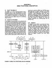
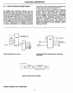
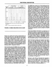
FIGURE 2·SA MC8-S0™
cPU
GROUP
DATA/ADDRESS
BUS
ADDRESS
components with improved
timing
margins and
access requirements.
(See
Figure
2-8.)
To enhance the system integration
of
MCS-85,
several special
components
with
combined
memory and
I/O
were designed. These new
devices
directly interface
to
the multiplexed
bus
of
the 8085A. The pin locations
of
the 8085A
and the special peripheral components are
assigned
to
minimize
PC
board area and
to
allow
for
efficient
layout. The
details
on
peripheral components are contained in subse-
quent
paragraphs
of
this
chapter
and in
Chapters 5 and
6.
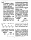
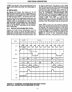
INTR-·----I
INTA
-----<II
RESET IN
--------I
RESET OUT
-------I
SOSSA
ADDRESS BUS
1---_
ALE
MULTIPLEXED
ADDRESS/DATA
BUS
IC>---
AD
10---
WR
1----
IO/M
FIGURE 2·SB MCS·S5™ cPU/SOS5A
(MCS-SO
COMPATIBLE
FUNCTIONS)
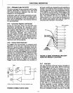
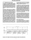
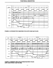
DATA IN
OR
OUT
= =
)(
__
A7_.AO_...JX
___
~_·D_o
__
L
TIME MULTIPLEX DATA
BUS
FIGURE
2·SC
MULTIPLEXED BUS
TIMING
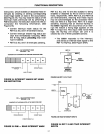
FIGURE 2·8 BASIC
CPU
FUNCTIONS
2-6