SYSTEM OPERATION
devices in the system, which would force them
to
be either ones or zeroes. Remember that
two
devices may not be selected simultaneously;
thus
each device must have an address that not
only selects itself, but also deselects all other
devices.
If
there are any bits which are truly
"don't
cares," they are customarily assigned
to
be zero. If all the
"X"
bits in Figure 3.1A were
"don't
cares," then the chip could
be
addressed
as memory locations
0-2k,
and
1/0
Ports
0-3.
Figure
3.1
B shows a slightly larger system
of
two
8355s
and
one
8156.
Notice that
8355
No.1
uses
its
two chip enable lines
to
decode
A12
=
1,
A
13
=
O.
It
is
possible
to
address each of the
chips without selecting any
of
the others. Also
notice that there are some illegal addresses
(e.g.,
A12
=
0,
A
13
=
1)
that would cause
two
of
the
devices
to
turn on simultaneously. The pro-
grammer must not use these addresses.
Figure 3.1C shows a larger MCS-85 system. Two
8205s are used
to
completely decode the ad-
dresses. There are some interesting points
to
observe here. First, while some
of
the devices
have
multiple possible address
(Le.,
they have
some
"don't
care" bits), there aren't any ad-
dresses which can cause simultaneous
selec-
tion
of
two or more parts. Second, the
1/0
and
FIGURE 3·2A SINGLE CHIP
8355/8755A
A,,---------tCE
vee----~CE
A'5
---------tIO/M
FIGURE 3·2B MULTIPLE CHIPS
8156
CE
101M
8355/8755A
CE
CE
101M
8355/8755A
-
memory portions
of
the 8x55 components share
chip enables, so they are forced
to
live with
each other's constraints. Third,
only one 8205 is
required per eight chips for the decoding;
that's
an overhead
of
only 1/8
of
a chip per part.
Figure
3.1
D shows a remedy
to
the problem il-
lustrated in Figure
3.1
C,
namely
that
I/O
and
memory portions
of
the chip are forced to live
with each other's chip enable constraints.
By
using a quad 2
to
1 multiplexer, the chip enables
of
the
I/O
and memory portions
of
four chips
can
be
independently assigned.
3.4.2
Memory·Mapped
110:
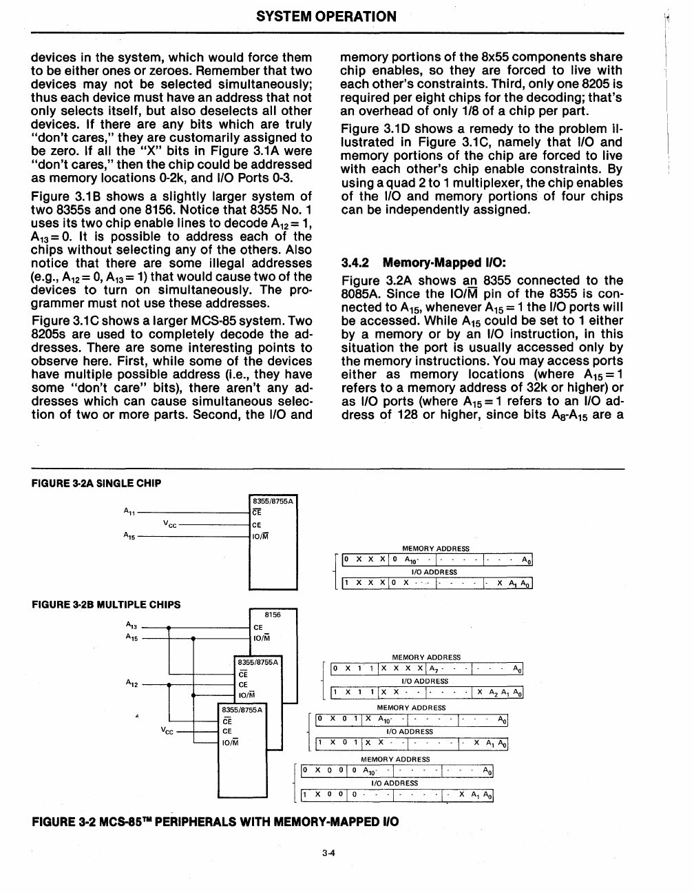
Figure 3.2A shows
all
8355 connected
to
the
8085A. Since the
101M
pin
of
the 8355 is con-
nected
to
A
15
, whenever A
15
= 1 the
1/0
ports will
be
accessed. While A
15
could be set
to
1 either
by a memory or by
an
I/O
instruction, in this
situation the port is
usually accessed only by
the memory instructions. You may access ports
either as memory locations (where A
15
= 1
refers
to
a memory address
of
32k
or
higher) or
as
1/0
ports (where A
15
= 1 refers
to
an
110
ad-
dress
of
128
or higher, since
bits
Aa-A15
are a
MEMORY ADDRESS
{
10
X X X I 0
A,o'
.
I·
. . .
I·
1/0 ADDRESS
11
X X
xlo
X ·-·-1- X
A,Aol
MEMORY ADDRESS
t
l
lox
1 1 I X X X X I A
7
- . . I .
1/0
ADDRESS
11
X 1 1 1 X X . .
I·
. . . I X
A2
A,
Aol
MEMORY ADDRESS
CE
Vee
CE
"---
101M
-
{
IO
X 0
11
x
A
la
-
-1-
..
-1-
. - Aol
1/0 ADDRESS
11
X 0 1 I X X .
·1-
- . .
I·
X
A,
Aol
MEMORY ADDRESS
1
1
{
:
X 0 0 I
'A,,"
"I"
" "
"I"
" "
"'I
1/0
ADDRESS
X 0 0 1
o·
. . I . . I: X
A,
Aol
FIGURE 3-2 MC8-8S™ PERIPHERALS WITH MEMORY-MAPPED
1/0
3-4
