In
general, tAD MEM and tLDR MEM are the parameters
needed for chip enabling, selection and address access
times,
and
probably are the most important considerations
when determining which memory device to
use.
When there
is
an
output enable, tRD MEM
is
also used. All relevant access
times must
be
met by the resulting system configuration to
be
compatible.
This note will not attempt to generalize a procedure that deals
with
the
interface to dynamic RAM, but the
2117
example
shown earlier
is
described below.
In
the dynamic RAM sys-
tem, many variables come into play upon which the memory
access is dependent. Among these are refresh controllers,
decoding, whether or not the system is designed for minimum
hardware or maximum performance, and consideration for
nonmultiplexed vs. multiplexed address dynamic RAMs.
For the Intel 2107C, which has nonmultiplexed addresses,
tAD is
the
important parameter as it generates the chip selects
and chip enables. However, with a multiplexed address part,
things
are
different and both a RAS and CAS access time
must
be
considered. Note that since
RAS
is applied before
CAS,
RAS
access time is effective only while the CAS signal
stays within the specified RAS to CAS delay time. If it is not
possible to do this, CAS access becomes the limiting factor
for memory selection. Don't be mislead by the
RAS
to CAS
maximum delay (tRCD:
RAS
to CAS delay time) spec'd on
dynamic RAM data sheets! This maximum only applies to
guarantee RAS access.
For a specific example the following shows how the speed
versions were selected for previous
2117
dynamic RAM inter-
face.
RAS path (from ALE)
5 gates
1 Flip Flop
(return path) 2 8216s
CAS path (from ALE)
3 gates
1
Flip Flop
4 D Flip Flops
approximate delay
7 ns
ea
15 ns
25 ns
ea
approximate delay
7 ns ea
15 ns
41
ns ea
tACCESS AVAILABLE FOR RAS =
tLDR - 5(7) -
15
- 2(25) = 360 ns
tACCESS AVAILABLE FOR CAS =
tLDR - 3(7) -
15
- 4(41) - 2(25) =
210
ns
Since
RAS
available time - CAS available time is greater
than the spec value for RAS to CAS delay on
~117
specs,
CAS access becomes the limiting factor. A CAS access of
165ns of the
2117-4
is well within the time available.
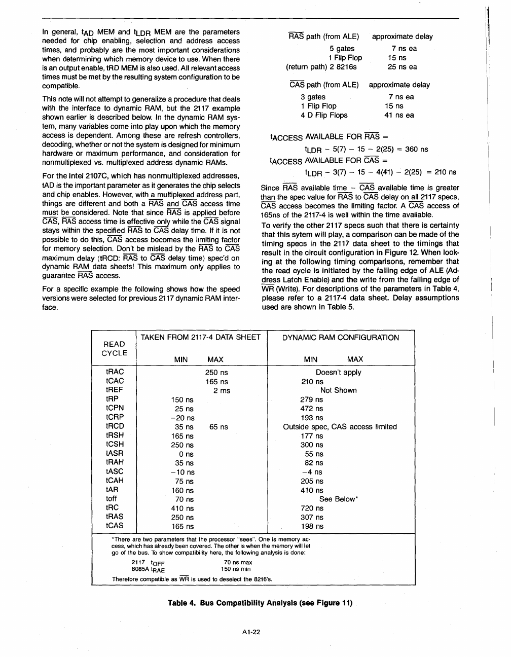
To verify the other 2117 specs such that there is certainty
that
this
sytem will play, a comparison can be made
of
the
timing specs in the 2117 data sheet to the timings that
result in the circuit configuration in Figure
12.
When look-
ing at the following timing comparisons, remember that
the read cycle is initiated by the falling edge
of
ALE
(Ad-
dress Latch Enable) and the write from the falling edge
of
WR (Write). For descriptions
of
the parameters in Table
4,
please refer
to
a
2117-4
data sheet. Delay assumptions
used are shown in Table
5.
'There
are two parameters that the processor "sees". One is memory ac-
cess, which has already been covered. The other is when the memory will let
go of the bus.
To
show compatibility here, the following analysis is done:
2117
tOFF 70
ns
max
8085A tRAE 150
ns
min
Therefore
compatible
as
WR
is used
to
deselect the 8216's.
Table
4.
Bus Compatibility Analysis (see Figure
11)
A1-22
